High-speed cross-coupled sense amplifier

a cross-coupled sense amplifier and high-speed technology, applied in pulse manipulation, pulse technique, instruments, etc., can solve the problems of slow divergence of potentials on data lines, disadvantage of a comparatively slow amplification speed, and no additional current supplied

Inactive Publication Date: 2005-04-26
LAPIS SEMICON CO LTD
View PDF4 Cites 17 Cited by
  • Summary
  • Abstract
  • Description
  • Claims
  • Application Information

AI Technical Summary

Benefits of technology

[0009]If the data lines are precharged to the power-supply level and then one of the data lines is driven toward a lower level, the first pair of n-channel MOS transistors reacts immediately to the

Problems solved by technology

The potentials on the data lines diverge slowly, because of limited driving capability of the transistors in the memory cell.
This type of cross-coupled sense amplifier has the advantage of low power consumption, but the disadvantage of a comparatively slow amplification speed.
In this scheme, however, the p-cha

Method used


Image

  • High-speed cross-coupled sense amplifier
  • High-speed cross-coupled sense amplifier
  • High-speed cross-coupled sense amplifier

Examples


Embodiment Construction

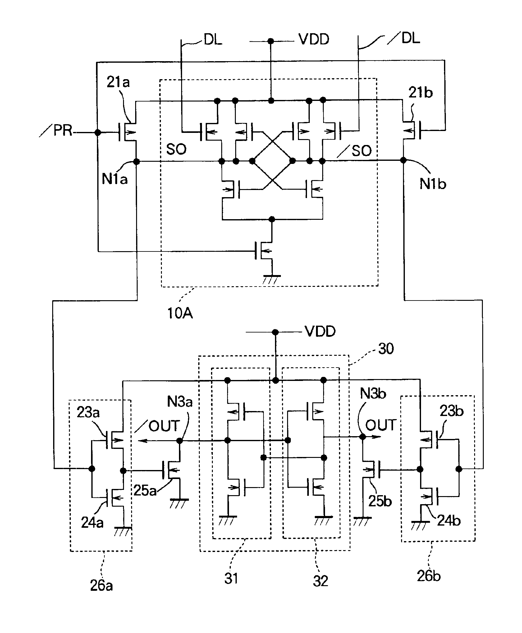
[0014]Embodiments of the invention will be described with reference to the attached drawings, in which like elements are indicated by like reference characters. The embodiments are sense amplifiers useful in SRAM and other semiconductor memory devices.

[0015]In the following description, language such as ‘A is connected to B through transistor C’ means either that the source of transistor C is connected to A and the drain of transistor C is connected to B, or the source of transistor C is connected to B and the drain of transistor C is connected to A. Similarly, to say that transistor C is controlled by D means that the gate of transistor C is connected to or receives D.

[0016]Referring to FIG. 1, a first embodiment has an amplifier circuit 10 connected to a pair of data lines DL and / DL, the slash indicating that the signal on data line / DL is complementary to the signal on data line DL. The amplifier circuit 10 comprises n-channel MOS transistors (NMOS transistors) 11a, 11b, 12a, 12...


PUM


Abstract

A sense amplifier has a pair of internal nodes that are precharged to a power-supply level. A first pair of n-channel transistors supplies current to the internal nodes responsive to a pair of data signals, both of which are initially high. When one of the data signals begins falling toward the low level, the corresponding n-channel transistor immediately reduces the current supplied to one of the internal nodes. A second pair of n-channel transistors, cross-coupled to the internal nodes, amplifies the resulting potential difference between the internal nodes, thereby pulling down the potential of one of the internal nodes. An output signal is generated from one or both of the internal nodes. The output signal is obtained quickly, because amplification begins without delay.

Description

BACKGROUND OF THE INVENTION[0001]1. Field of the Invention[0002]The present invention relates to a sense amplifier for use in a semiconductor memory such as a static random access memory (SRAM).[0003]2. Description of the Related Art[0004]An SRAM memory cell outputs complementary data signals on a pair of data lines that have been precharged to equal potentials. The potentials on the data lines diverge slowly, because of limited driving capability of the transistors in the memory cell. It is known art to use a pair of complementary metal-oxide-semiconductor (MOS) inverters cross-coupled to the data lines as a sense amplifier to amplify the potential difference so that the data can be read quickly. This type of cross-coupled sense amplifier has the advantage of low power consumption, but the disadvantage of a comparatively slow amplification speed.[0005]It is also known art to speed up the amplification process by having a pair of p-channel MOS transistors supply additional current t...

Claims


Application Information

Patent Timeline
IPC IPC(8): G01R19/00G11C11/419H03K5/22H03F3/45G11C7/06H03K5/24
CPCG11C7/062H03K5/249H03K5/2481G11C7/065
Inventor SATO, YUKIO
Owner LAPIS SEMICON CO LTD
Why Eureka
Try Eureka