Diode for use in MRAM devices and method of manufacture

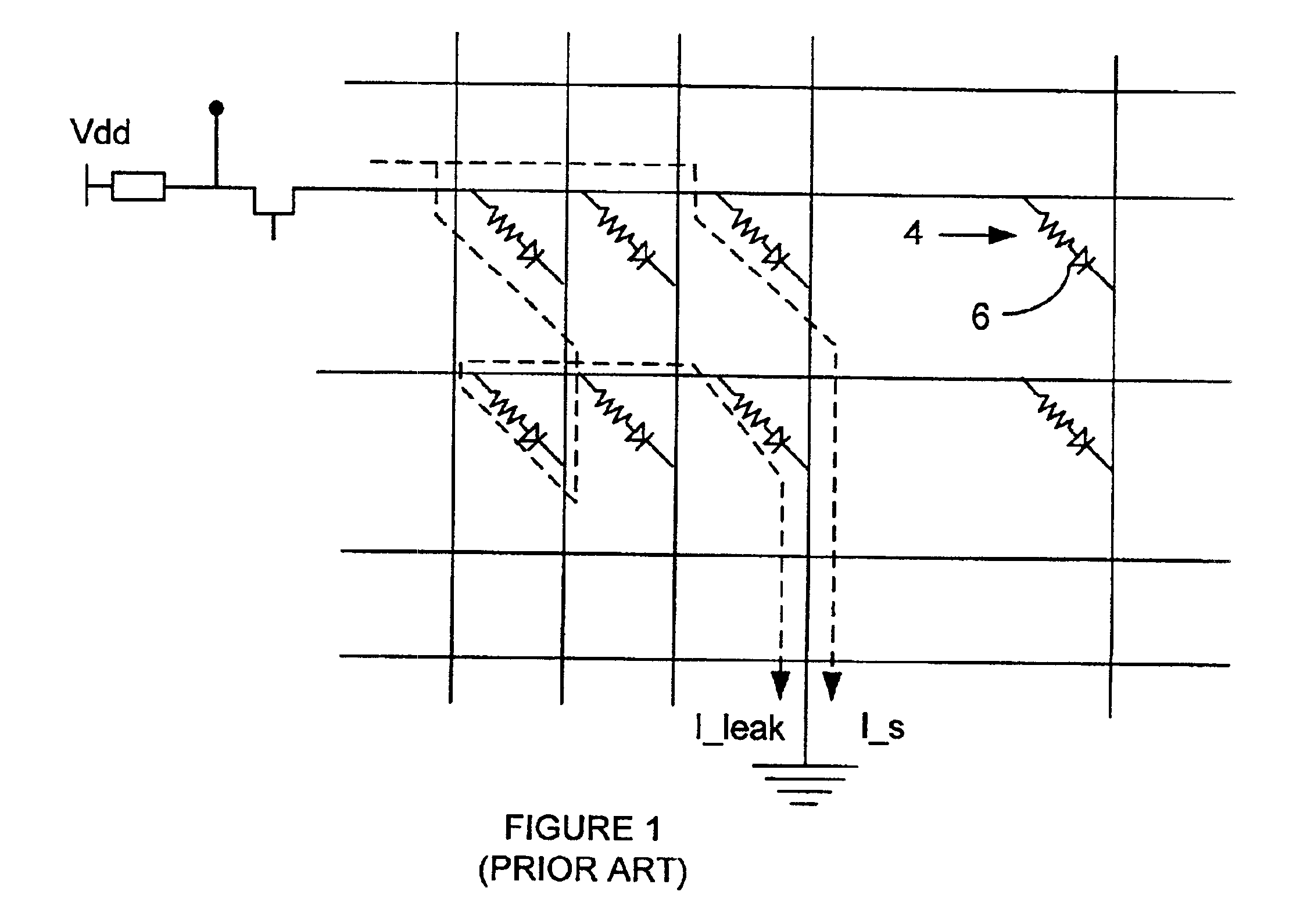
a technology of mram devices and diodes, applied in semiconductor devices, digital storage, instruments, etc., can solve the problems of obscuring the sense current, unable to reliably detect the resistance state of a single memory cell in an array, and compact mram devices that consume less power than other conventional storage devices

Inactive Publication Date: 2005-04-26
SAMSUNG ELECTRONICS CO LTD
View PDF20 Cites 41 Cited by
  • Summary
  • Abstract
  • Description
  • Claims
  • Application Information

AI Technical Summary

Problems solved by technology

In addition, the MRAM devices are more compact and consume less power than other conventional storage devices.
Sensing the resistance state of a single memory cell in an array, however, can be unreliable.
The parasitic or leakage current becomes large in a large array and, therefore, can obscure the sense current.
Unreliability in sensing the resistance state is compounded by manufacturing variations, v

Method used


Image

  • Diode for use in MRAM devices and method of manufacture
  • Diode for use in MRAM devices and method of manufacture
  • Diode for use in MRAM devices and method of manufacture

Examples


Embodiment Construction

[0022]Reference will now be made to the exemplary embodiments illustrated in the drawings, and specific language will be used herein to describe the same. It will nevertheless be understood that no limitation of the scope of the invention is thereby intended. Alterations and further modifications of the inventive features illustrated herein, and additional applications of the principles of the inventions as illustrated herein, which would occur to one skilled in the relevant art and having possession of this disclosure, are to be considered within the scope of the invention.

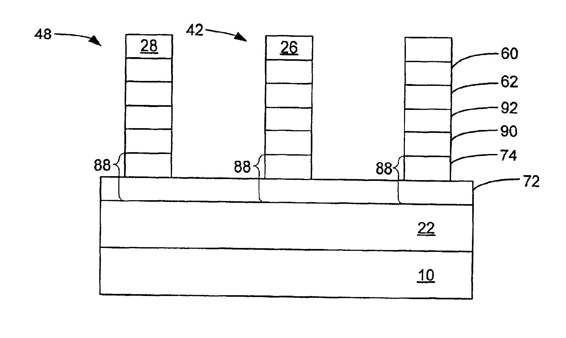
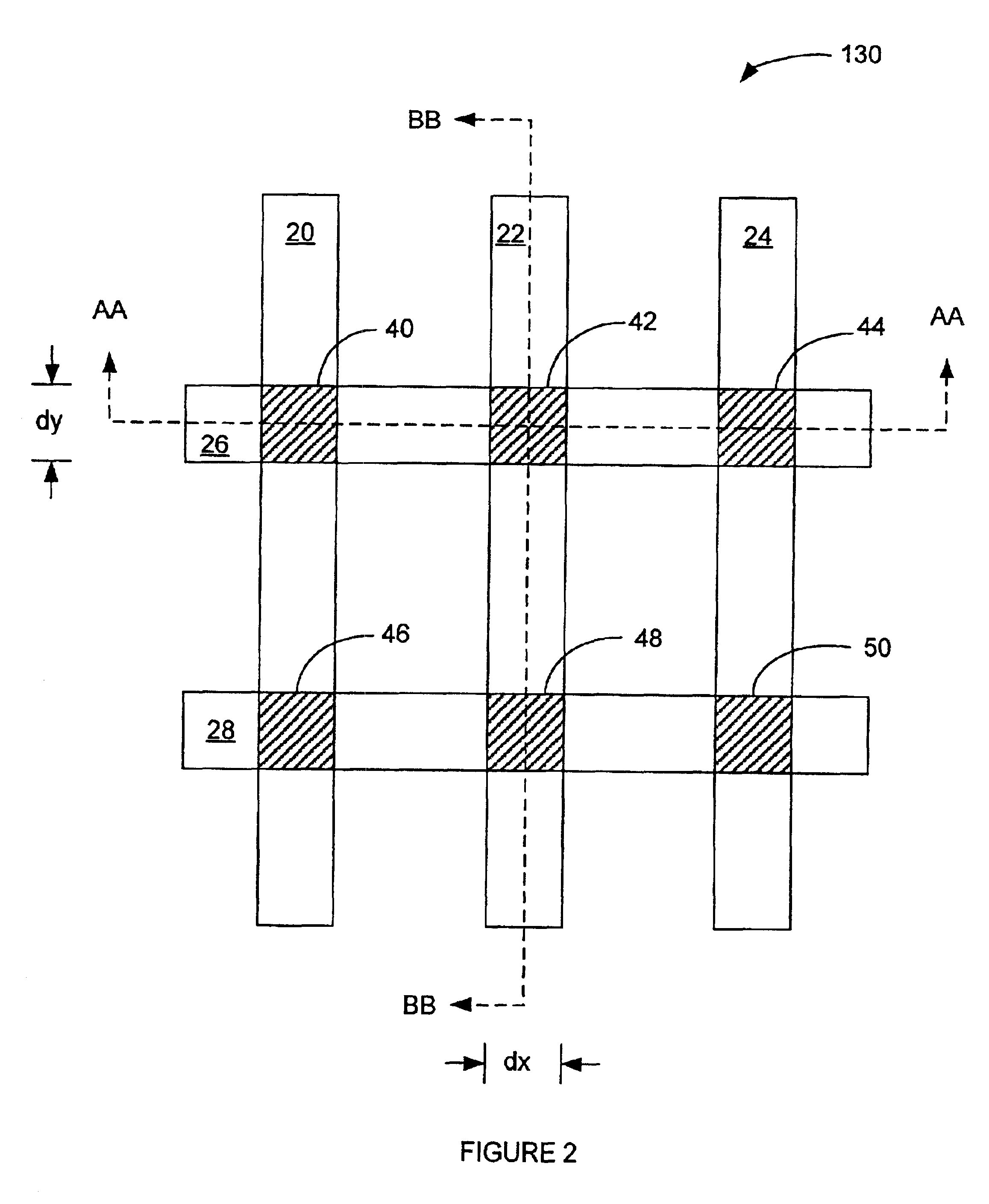
[0023]As shown in the drawings for purposes of illustration, the present invention is embodied in a magnetic random access memory device. The MRAM device includes an array of memory cells and a read-write circuit for reading or writing data from the memory cells. The read circuit, which includes equipotential application devices and differential sensing amplifiers, can reliably sense different resistance states o...


PUM


Abstract

A data storage device is disclosed that has a plurality of word lines, a plurality of bit lines, and a resistive crosspoint array of memory cells. Each memory cell is connected to a bit line and connected to an isolation diode that further connects to a respective word line. The isolation diode provides a unidirectional conductive path from the bit line to the word line. Each word line provides a common metal-semiconductor contact with each diode sharing the word line such that each diode has a separate metal contact located between the semiconductor portion of the common metal-semiconductor contact and its respective memory cell.

Description

BACKGROUND OF THE INVENTION[0001]The present invention relates generally to random access memory for data storage. More specifically, the present invention relates to a magnetic random access memory device that includes improved unidirectional elements to limit leakage current within the array.[0002]Magnetic random access memory (“MRAM”) is a non-volatile memory that shows considerable promise for long-term data storage. Performing read and write operations on MRAM devices are much faster than performing read and write operations on conventional memory devices such as DRAM and Flash and order of magnitude faster than long-term storage devices such as hard drives. In addition, the MRAM devices are more compact and consume less power than other conventional storage devices.[0003]A typical MRAM device includes an array of memory cells. Word lines extend across rows of the memory cells and bit lines extend along columns of the memory cells. Each memory cell is located at a crosspoint of...

Claims


Application Information

Patent Timeline
IPC IPC(8): G11C11/15G11C11/00G11C11/16G11C11/02H01L21/8246H01L27/105H01L43/08
CPCG11C11/00H01L27/224G11C11/16G11C11/15G11C11/1659G11C11/1657H10B61/10
Inventor SHARMA, MANISHTRAN, LUNG T.
Owner SAMSUNG ELECTRONICS CO LTD
Why Eureka
Try Eureka