Patterned oxygen and moisture absorber for organic optoelectronic device structures

a technology of organic optoelectronic devices and oxygen and moisture absorbers, which is applied in the manufacture of electrode systems, electric discharge tubes/lamps, and discharge tubes luminescnet screens, etc., can solve the problems of severe limit the lifetime of the devices, and the obstructing of the transmission of light to the outer environment of the getter

Inactive Publication Date: 2005-05-03
UNIVERSAL DISPLAY
View PDF24 Cites 89 Cited by
  • Summary
  • Abstract
  • Description
  • Claims
  • Application Information

AI Technical Summary

Benefits of technology

[0019]An advantage of the present invention is that organic optoelectronic device structures are provided that are effective in protecting certain sensitive components of the structures from oxygen, moisture and other harmful species in the surrounding atmosphere.
[0020]Another advantage of the present invention is that top emitting and transparent OLED structures are provided that afford protection from these harmful species.
[0021]Yet another advantage of the present invention is that flexible OLED structures are provided that afford protection from these harmful species.
[0022]These and other embodiments and advantages of the present invention will become readily apparent to those of ordinary skill in the art upon review of the disclosure to follow.

Problems solved by technology

Unfortunately, certain OLED structure components, such as reactive metal cathode components, are susceptible to oxygen and moisture, which exist in the ambient atmosphere and can produce deleterious effects that can severely limit the lifetime of the devices.
However, due to the fashion in which the getter material is disposed inside the cover, if this device design were to be used in connection with a top-emitting or transparent OLED configuration, then the getter would obstruct the transmission of light to the outer environment.

Method used


Image

  • Patterned oxygen and moisture absorber for organic optoelectronic device structures
  • Patterned oxygen and moisture absorber for organic optoelectronic device structures
  • Patterned oxygen and moisture absorber for organic optoelectronic device structures

Examples


Embodiment Construction

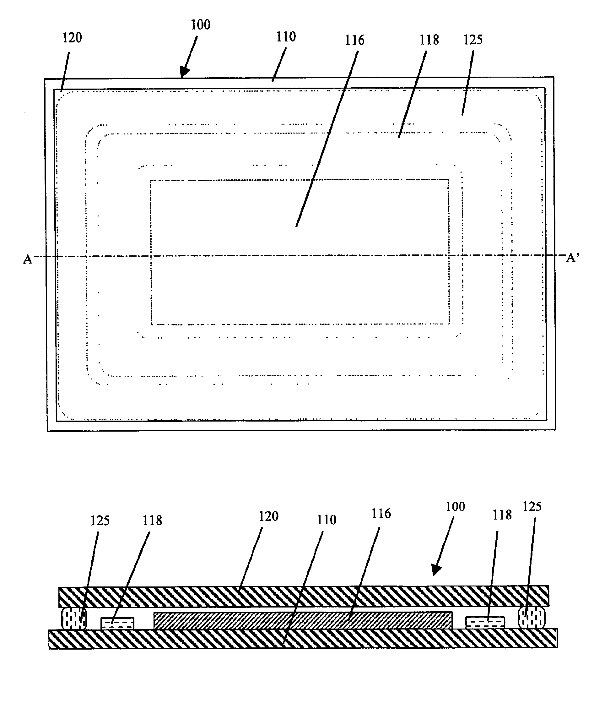
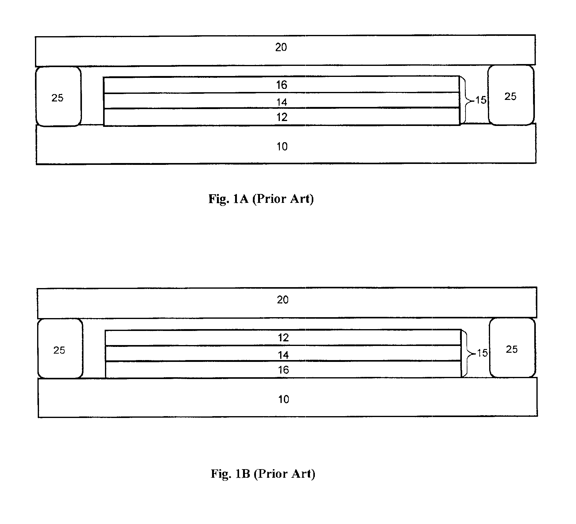
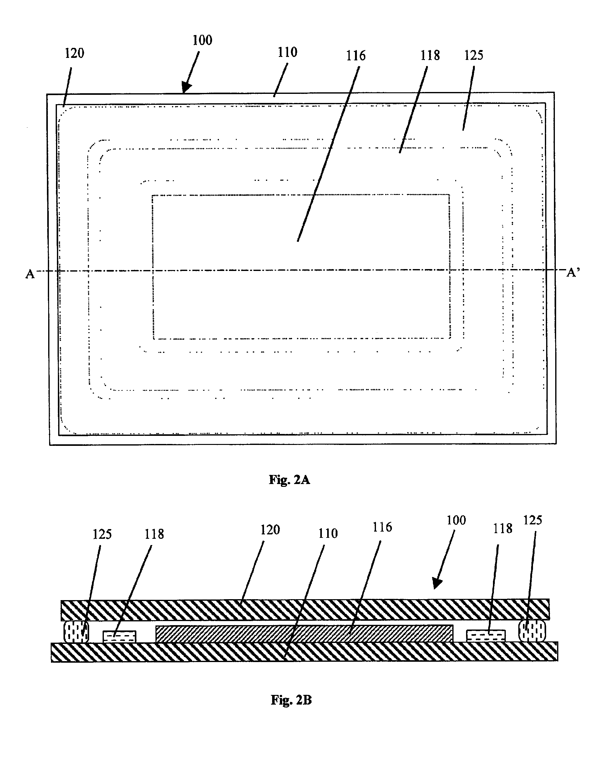
[0029]The present invention now will be described more fully hereinafter with reference to the accompanying drawings in which preferred embodiments of the invention are shown. This invention may, however, be embodied in different forms and should not be construed as limited to the embodiments set forth herein. For example, the drawings are directed to OLED structures, but other optoelectronic structures, such organic phototransistor structures, organic photodetector structures, and organic photovoltaic device structures are also contemplated.

[0030]As used herein, a “layer” of a given material includes a region of that material whose thickness is small compared to both its length and width. Examples of layers include sheets, foils, films, laminations, coatings, and so forth. As used herein a layer need not be planar, but can be bent, folded or otherwise contoured, for example, to at least partially envelop another component. As used herein a layer can also include multiple sub-layers...


PUM

PropertyMeasurementUnit
thicknessaaaaaaaaaa
thicknessaaaaaaaaaa
transmissionaaaaaaaaaa

Abstract

An OLED device structure and a method of making the same. The OLED device structure comprises (a) a substrate, (b) an OLED display area comprising one or more active pixels disposed over the substrate, wherein each of the one or more active pixels comprises an anode region, a cathode region and a light-emitting region, (c) a cover over the OLED display area, wherein the cover permits transmission of light from the one or more active pixels and an outer environment, and wherein the cover and the substrate cooperate to restrict transmission of oxygen and water vapor from the outer environment to the OLED display area, and (d) a patterned getter layer disposed between the substrate and the cover, wherein the patterned getter layer is configured so as to substantially avoid obstructing the transmission of light from the one or more pixels. Also disclosed are a flexible OLED device and an organic optoelectronic device structures having related configurations.

Description

FIELD OF THE INVENTION[0001]The present invention relates to structures that protect organic optoelectronic devices from species in the surrounding environment.BACKGROUND OF THE INVENTION[0002]Organic optoelectronic devices, including organic light emitting devices, organic phototransistors, organic photodetectors, and organic photovoltaic devices, are known in the art and are frequently used in connection with multi-device arrays.[0003]For example, organic light emitting devices (“OLEDs”), including both polymer and small-molecule OLEDs, are potential candidates for a great variety of virtual- and direct-view type displays, such as lap-top computers, televisions, digital watches, telephones, pagers, cellular telephones, calculators and the like. Unlike inorganic semiconductor light emitting devices, organic light emitting devices are generally simple and are relatively easy and inexpensive to fabricate. Also, OLEDs readily lend themselves to applications requiring a wide variety of...

Claims


Application Information

Patent Timeline
Patent Type & Authority Patents(United States)
IPC IPC(8): H01L51/52H01L51/50
CPCH01L51/5237Y10T428/231H10K59/10H10K59/12H10K50/846
Inventor SILVERNAIL, JEFFREY ALANWEAVER, MICHAEL STUART
Owner UNIVERSAL DISPLAY
Why Eureka
Try Eureka