Tunable optical add/drop multiplexer with multi-function optical amplifiers

a multi-functional optical amplifier and add/drop technology, applied in the field of integrated photonic circuits, can solve the problems of many photonic functional blocks that are not monolithically integrated together and are discr

Inactive Publication Date: 2005-05-03
MASSACHUSETTS INST OF TECH
View PDF14 Cites 42 Cited by
  • Summary
  • Abstract
  • Description
  • Claims
  • Application Information

AI Technical Summary

Problems solved by technology

Currently, many photonic functional blocks are discrete and are not monolithically integrated together.

Method used


Image

  • Tunable optical add/drop multiplexer with multi-function optical amplifiers
  • Tunable optical add/drop multiplexer with multi-function optical amplifiers
  • Tunable optical add/drop multiplexer with multi-function optical amplifiers

Examples


second embodiment

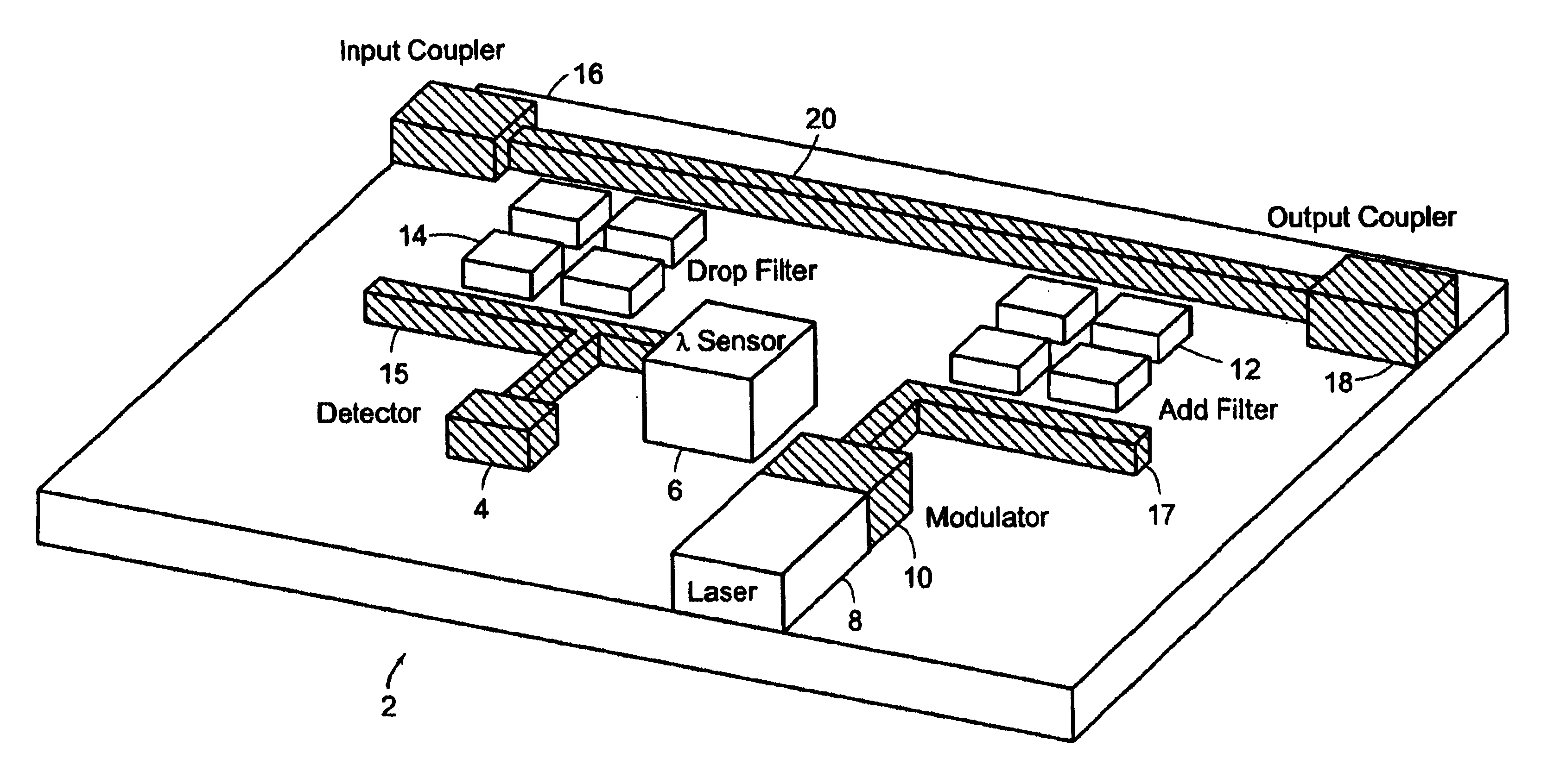
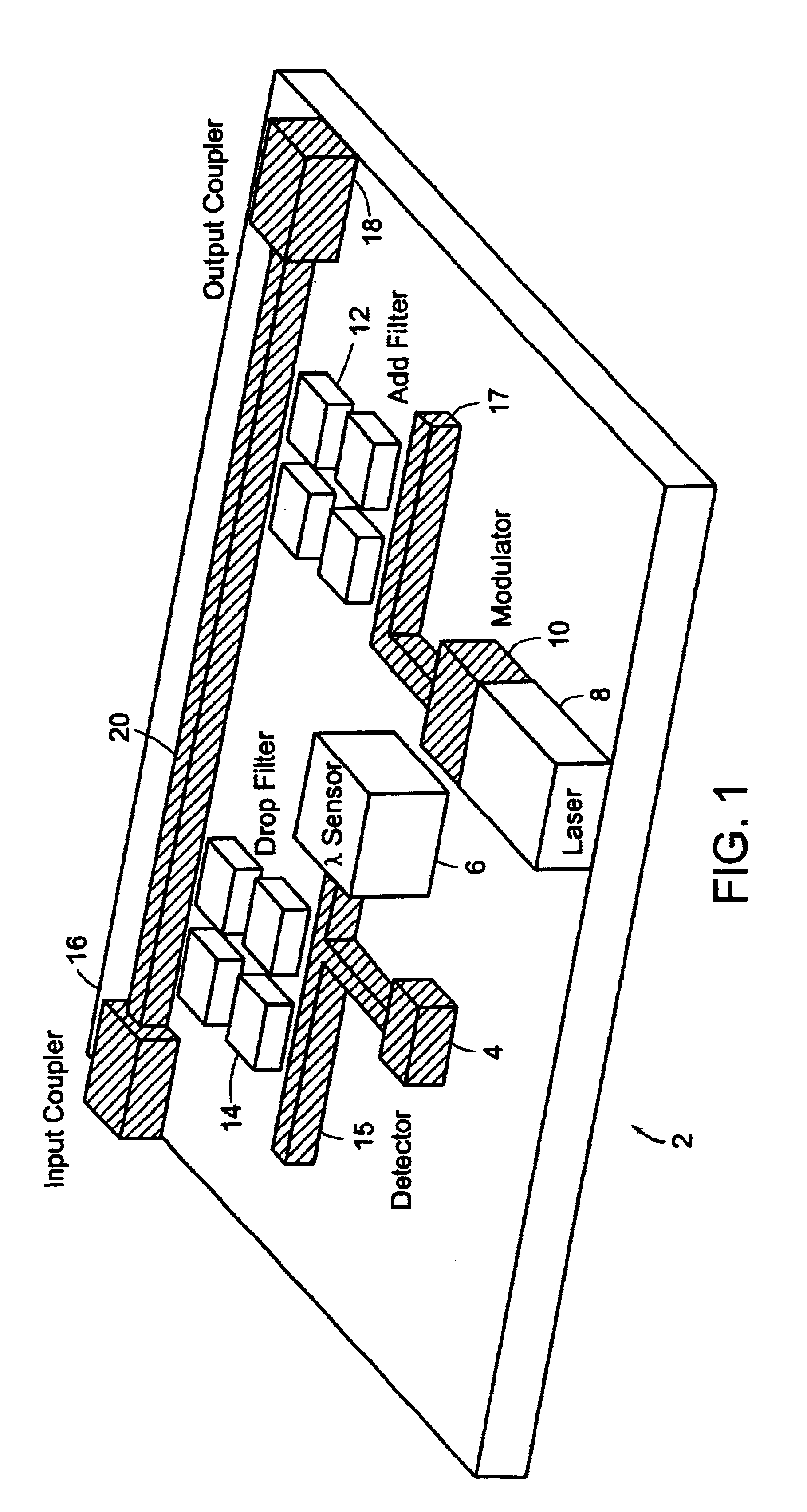
[0042]Since the SOA can amplify or absorb light, the SOA structure can also be used as a modulator. In one embodiment, by modulating the electrical bias on a SOA, the SOA can either absorb light or transmit / amplify light. In a second embodiment, an SOA can be used to modify the phase of the light traveling through one arm of a Mach-Zenhder interferometer. Using the SOA to change the phase of the light by 180 degrees, the light will destructively intefere with the light being transmitted through the other arm of the interferometer. Hence, the intensity of the light being transmitted through the interferometer can be modulated.

[0043]A SOA can be fabricated in two different configurations as shown in FIGS. 4A and 4B. FIG. 4A shows a vertical cavity semiconductor optical amplifier (VCSOA) 42. The VCSOA 42 includes an upper 48 and a lower 52 distributed Bragg reflectors, an active region 50, an upper 46 and a lower 54 cladding layers, and metal contacts 44 and 56. Moreover, the VCSOA 42 ...

third embodiment

[0086]In the invention, the photonic integrated circuit is fabricated on a GaAs substrate using an in-plane SOAs designed to operate at wavelengths near 1300 nm as similarly shown in FIGS. 8A and 8B. Also, the passive waveguide includes a high dielectric constant material, such as GaAs, while the active waveguide includes InGaAsN quantum wells or InAs quantum dots embedded in InGaAs that are cladded with an InGaAsP alloy. Within the waveguides that route the light from one functional block to the next, the passive waveguide is separated from the active waveguide by a layer of oxidized AlAs. The high index contrast between the passive waveguide and adjacent aluminum oxide keeps the light confined within the passive waveguide and prevents its interaction with the active waveguide.

[0087]The SOA of this embodiment includes active and passive waveguides surrounded by cladding material. The cladding material can be composed of an (In, Ga, Al) (As, P) alloy that has a low dielectric consta...

fourth embodiment

[0091]In the invention, the photonic integrated circuit is fabricated on an InP substrate using SOAs designed to operate at wavelengths between approximately 1300 nm and 1600 nm as similarly shown in FIGS. 8A and 8B. The passive waveguide includes a high dielectric material, such as InGaAsP, with a high As content, while the active waveguide includes InGaAsP quantum wells that are cladded with a second InGaAsP alloy. Within the waveguides that route the light from one functional block to the next, the passive waveguide is separated from the active waveguide by the AlAsSb layer. The high index contrast between the passive waveguide and the adjacent AlAsSb layers keeps the light confined within the passive waveguide and prevents its interaction with the active waveguide.

[0092]The SOA of this embodiment includes the active and passive waveguides surrounded by cladding material. The cladding material can be composed of an (In, Ga) (As, P) alloy as a low dielectric material, which surrou...


PUM


Abstract

A photonic circuit includes a tunable drop filter arrangement that includes a plurality of resonators. The drop filter arrangement is tuned to remove a selected frequency from an input data stream from a waveguide. A wavelength sensor coupled to the drop filter to monitor the selected frequency to which the drop filter arrangement has been tuned. A tunable laser presents a new signal of a defined frequency indicative of a signal to be added to the input data stream. A modulator coupled to the tunable laser for receiving the new signal and forming a modulated signal. An add filter arrangement coupled to the modulator for receiving the modulated signal and adding the modulated signal to the data stream.

Description

PRIORITY INFORMATION[0001]This application claims priority from provisional application Ser. No. 60 / 332,242 filed Nov. 14, 2001, the disclosure of which is incorporated herein by reference.BACKGROUND OF THE INVENTION[0002]The invention relates to the field of integrated photonic circuits including tunable add / drop filters, a detector, a wavelength sensor, a modulator, and a tunable laser for use in telecommunication systems and networks.[0003]Currently, many photonic functional blocks are discrete and are not monolithically integrated together. To create photonic circuits, hybrid integration approaches have been used when dealing with the integration of several functional blocks.[0004]The need to remove information from and add information to dense wavelength division multiplexing (DWDM) data streams can be vital to optical networks. Tunable add / drop filters allow any wavelength within the DWDM data stream to be extracted and allow the wavelength tobe added back into the DWDM data s...

Claims


Application Information

Patent Timeline
Patent Type & Authority Patents(United States)
IPC IPC(8): G02B6/12H01S5/50H01S5/00H01S5/34H01S5/0687H01S5/10H01S5/0625H01S5/183H01S5/026H01S3/063H01S3/23H01S5/40
CPCB82Y20/00H01S5/50G02B6/12007G02B6/12004G02B2006/12109H01S3/063H01S3/2383H01S5/02248H01S5/026H01S5/06256H01S5/0687H01S5/1032H01S5/1071H01S5/18311H01S5/1833H01S5/3412H01S5/4025H01S5/02325
Inventor KOLODZIEJSKI, LESLIEPETRICH, GALE S.
Owner MASSACHUSETTS INST OF TECH
Why Eureka
Try Eureka