System for probing, testing, burn-in, repairing and programming of integrated circuits
What is AI technical title?
AI technical title is built by PatSnap AI team. It summarizes the technical point description of the patent document.
a technology for integrated circuits and burn-in circuit devices, which is applied in the direction of semiconductor/solid-state device testing/measurement, semiconductor/solid-state device details, instruments, etc., can solve the problems of circuit device burn-in and circuit device testing that requires many hours of testing the device, and conventional probe cards do not provide the capability of contacting all the dice on a wafer. , to achieve the effect of reducing the thickness of oxide films
Inactive Publication Date: 2005-05-10
ELM TECH
View PDF110 Cites 28 Cited by
Summary
Abstract
Description
Claims
Application Information
AI Technical Summary
This helps you quickly interpret patents by identifying the three key elements:
Problems solved by technology
Method used
Benefits of technology
Benefits of technology
[0014]The objects, features and advantage of the present invention will be apparent from the following detailed description in which:
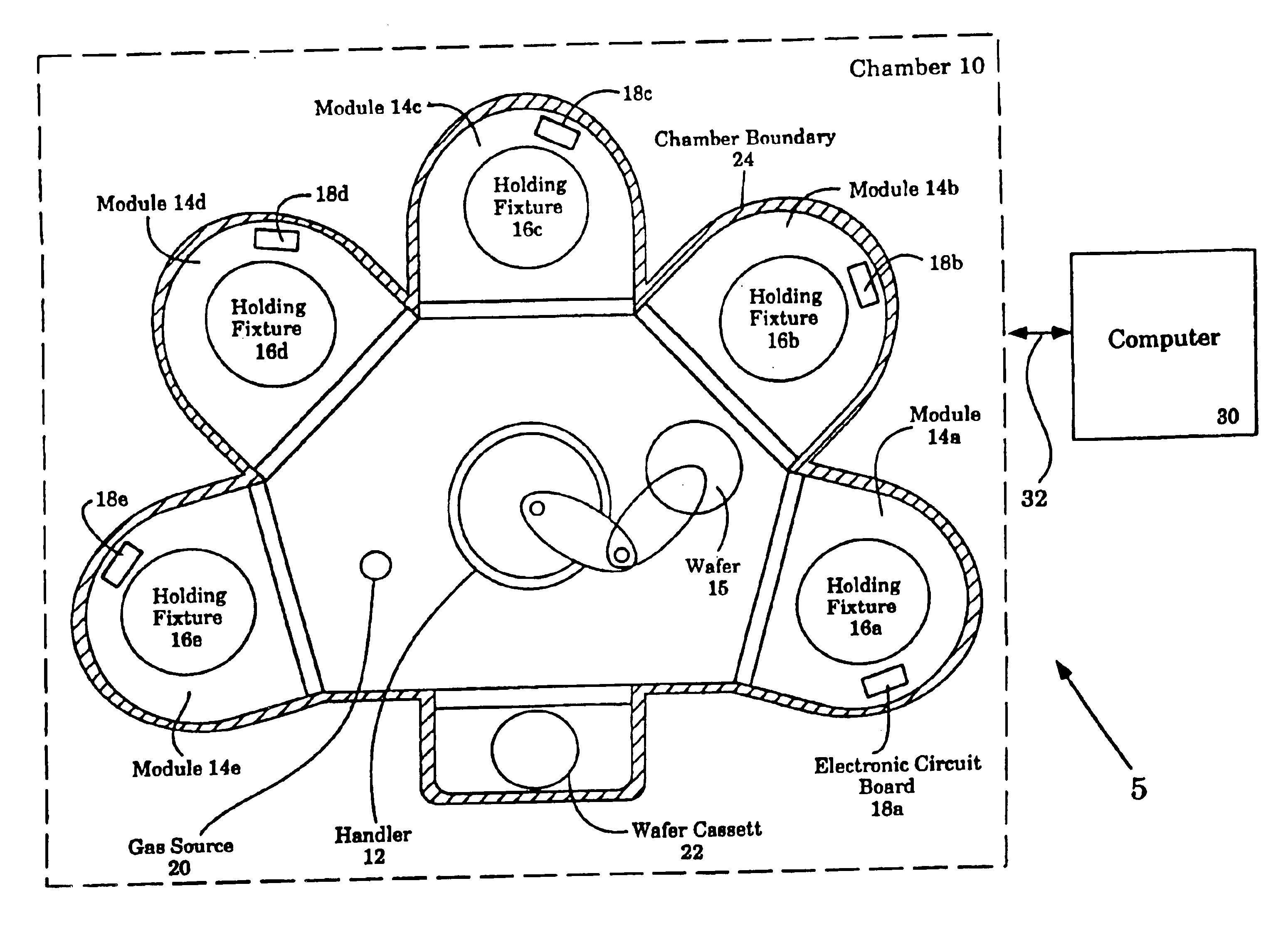
[0015]FIG. 1 is a multi-functional semiconductor test and circuit configuration system according to the present invention.
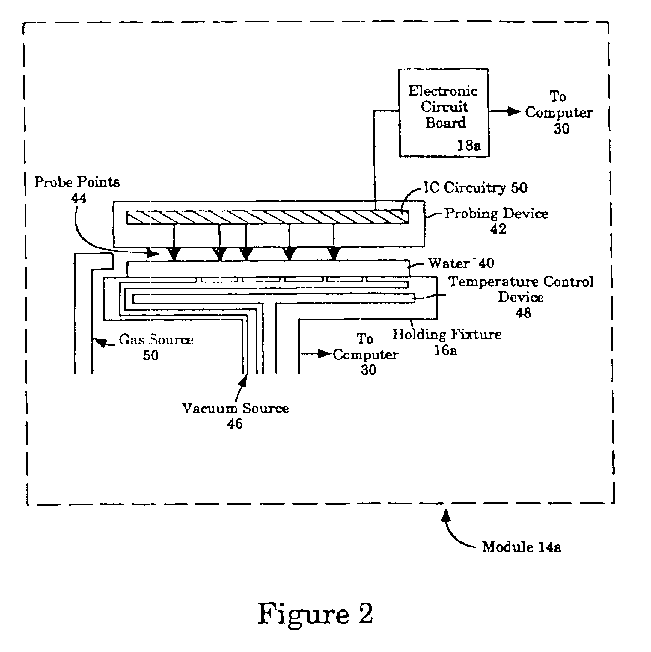
[0016]FIG. 2 is one of the modules shown in FIG. 1.
[0017]FIG. 3 is a wafer having a plurality of integrated circuits.
[0018]FIG. 4 is a flow chart illustrating the steps of reducing the thickness of oxide films on the contact pads of the integrated circuits and the steps of testing, burning-in, configuring and binning the integrated circuits according to the present invention.
[0019]FIG. 5 is a detailed block diagram of the computer shown in FIG. 1 according to one embodiment of the present invention.
Problems solved by technology
Conventional probe cards do not provide the capability of contacting all the dice on a wafer at once.
Burn-in of circuit devices requires many hours of testing the devices under stressing temperature and electrical conditions.
Method used
Image
Click on the blue label to locate the original text in one second.
Reading with bidirectional positioning of images and text.
Examples
Embodiment Construction
[0020]The present invention provides methods and apparatus for performing testing, burn-in, repairing, programming, and binning of integrated circuits in a closed environment using a single piece of equipment. In the following detailed description, numerous specific details are set forth such as particular hardware configurations and a flow chart to provide a thorough understanding of the present invention. It will be appreciated, however, by one having ordinary skill in the art that the present invention may be practiced without such specific details. In other instances, well-known structures and methods are not described to avoid obscuring the present invention unnecessarily.
[0021]Now referring to FIG. 1, a semiconductor test and circuit configuration system 5, which is a cluster tool, is presented according to one embodiment of the present invention. System 5 includes a chamber 10 and a computer 30. Chamber 10 includes a plurality of modules 14a-14e for processing wafers, a handl...
PUM
Property
Measurement
Unit
temperatures
aaaaa
aaaaa
temperature
aaaaa
aaaaa
thickness
aaaaa
aaaaa
Abstract
A system which performs multi-functions including reducing the thickness of oxides on contact pads and probing, testing, burn-in, repairing, programming and binning of integrated circuits. The system includes: at least one module having a holding fixture, a wafer, a probing device, an electronic circuit board, and a temperature control device. There are a number of integrated circuits on the wafer, and the probing device simultaneously contacts substantially all of the electrical contacts in the integrated circuits. There is a plurality of active switching circuits on the probing device. The module may also have a gas source for supplying non-oxidizing gases such as nitrogen and hydrogen into the chamber, a handler for moving the wafers and the probing devices, and a computer coupled to the chamber for controlling and communicating with the handler, the temperature control devices, the holding fixtures and the probing devices. The holding fixture holds a wafer having integrated circuits and aligns the wafer to a probing device. The temperature control device is used to heat the wafer during an oxide reduction process or during burn-in of the wafer. During an oxide reduction process, hydrogen is introduced into the chamber, and the wafer is heated so that the oxides on the contact pads can combine with hydrogen to form water vapor, thus reducing the thickness of the oxides. The computer analyzes the test and / or burn-in data and provides control signals for repairing or programming the integrated circuits. The computer system also generates a database that contains the performance data of all the integrated circuits on the wafer that are tested and allows for immediate feedback of the quality of the integrated circuits.
Description
CROSS-REFERENCE TO RELATED APPLICATIONS[0001]This application is a divisional of U.S. patent application Ser. No. 09 / 946,552 filed Sep. 6, 2001, now U.S. Pat. No. 6,838,896, incorporated herein by reference in its entirety, which is a divisional of Ser. No. 08 / 474,489 filed Jun. 7, 1995, U.S. Pat. No. 6,288,561; which is a CIP of Ser. No. 08 / 055,439 filed Apr. 30, 1993, U.S. Pat. No. 5,451,489; which is a divisional of Ser. No. 07 / 775,324 filed Oct. 11, 1991, U.S. Pat. No. 5,225,771; which is a divisional of Ser. No. 07 / 482,135 filed Feb. 16, 1990, U.S. Pat. No. 5,103,557; which is a CIP of Ser. No. 07 / 194,596 filed May 16, 1998, U.S. Pat. No. 4,924,589 and said Ser. No. 08 / 474,489 filed Jun. 7, 1995 is a CIP of Ser. No. 08 / 315,905 filed Sep. 30, 1994, U.S. Pat. No. 5,869,354; which is a divisional of Ser. No. 07 / 865,412 filed Apr. 8, 1992, U.S. Pat. No. 5,354,695 and said Ser. No. 08 / 474,489 filed Jun. 7, 1995 is a CIP of Ser. No. 08 / 217,410 filed Mar. 24, 1994, U.S. Pat. No. 5,453...
Claims
Application Information
Patent Timeline
Application Date:The date an application was filed.
Publication Date:The date a patent or application was officially published.
First Publication Date:The earliest publication date of a patent with the same application number.
Issue Date:Publication date of the patent grant document.
PCT Entry Date:The Entry date of PCT National Phase.
Estimated Expiry Date:The statutory expiry date of a patent right according to the Patent Law, and it is the longest term of protection that the patent right can achieve without the termination of the patent right due to other reasons(Term extension factor has been taken into account ).
Invalid Date:Actual expiry date is based on effective date or publication date of legal transaction data of invalid patent.

