Surface inspection apparatus and method thereof

Inactive Publication Date: 2005-05-17
HITACHI LTD +1
View PDF6 Cites 34 Cited by
  • Summary
  • Abstract
  • Description
  • Claims
  • Application Information

AI Technical Summary

Benefits of technology

[0017]According to the above-mentioned structure, the defect is discriminated between the very shallow small scratch and the foreign object that occur when the surface of an insulating film or the like of a sample is subjected to CMP process, and further i

Problems solved by technology

If scratches having various configuration are formed on the surface of a work target in the semiconductor manufacturing process or the magnetic head manufacturing process as described hereinabove, a scratch causes insufficient etching in wiring forming and causes the defect such as short-circuit.
Fu

Method used


Image

  • Surface inspection apparatus and method thereof
  • Surface inspection apparatus and method thereof
  • Surface inspection apparatus and method thereof

Examples


first embodiment

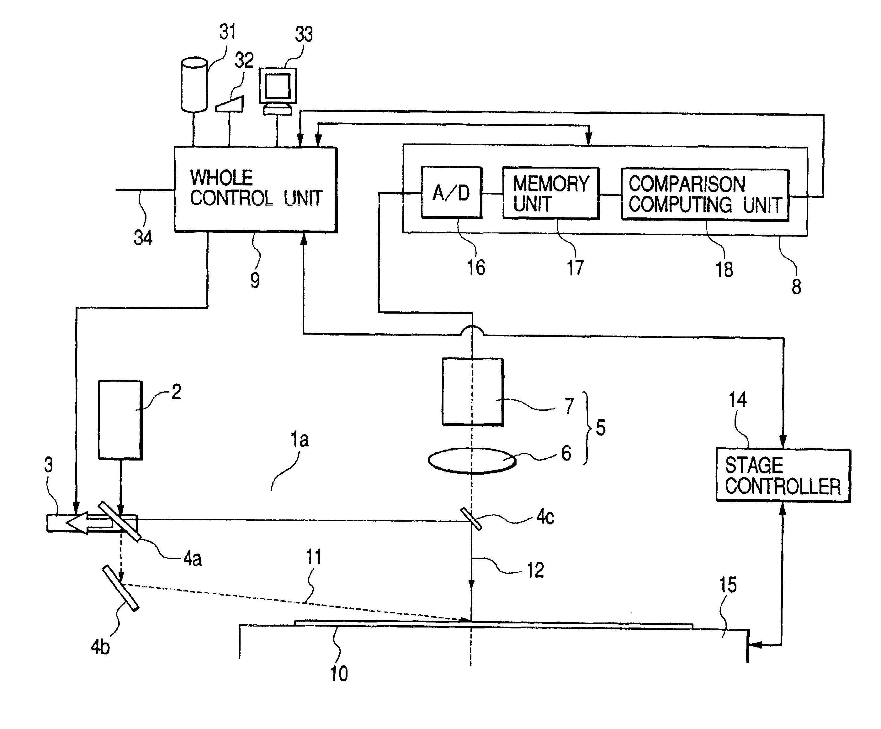
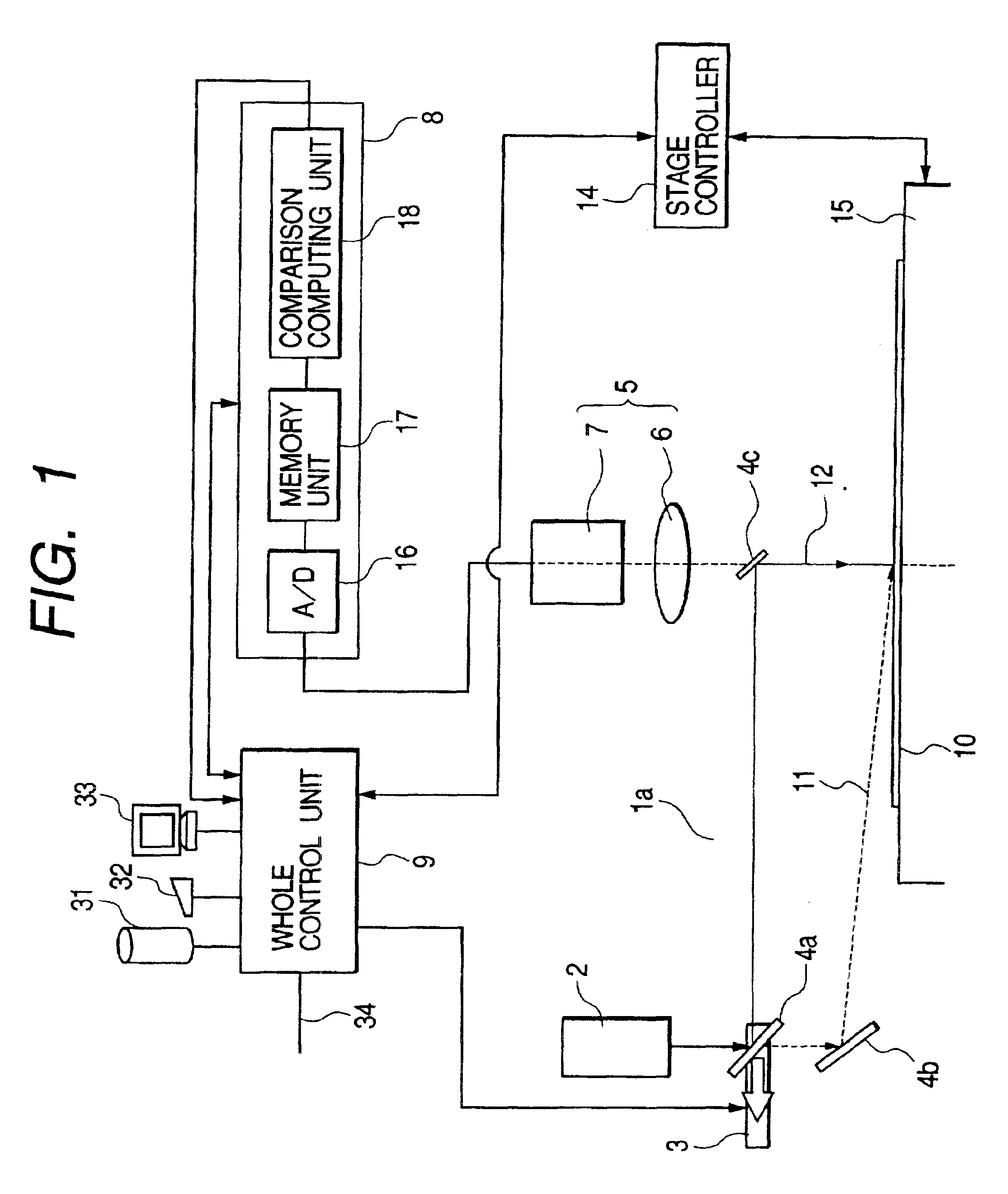
[0062]The first example of a surface inspection apparatus for inspecting the scratch or the like used for realizing the first embodiment will be described with reference to FIG. 1 to FIG. 9. In detail, as shown in FIG. 1, the surface inspection apparatus of the first example is provided with a wafer 10 that is an object to be inspected placed on a stage 15 controllably moved in X-Y direction based on the measured positional coordinate, an illumination optical system 1a comprising a light source 2 having a light source for emitting a light such as Ar laser of wavelength 488 nm (blue wavelength), nitrogen laser, He—Cd laser, or excimer laser (not limited to a laser light source), an optical path switching mechanism 3, and reflection mirrors 4a, 4b, and 4c, a detection optical system 5 comprising a condenser lens 6 and a photoelectric converter 7 having a photomultiplier, CCD camera, CCD sensor, or TDI sensor, a computation processing unit B comprising an A / D conversion unit 16 for con...

second embodiment

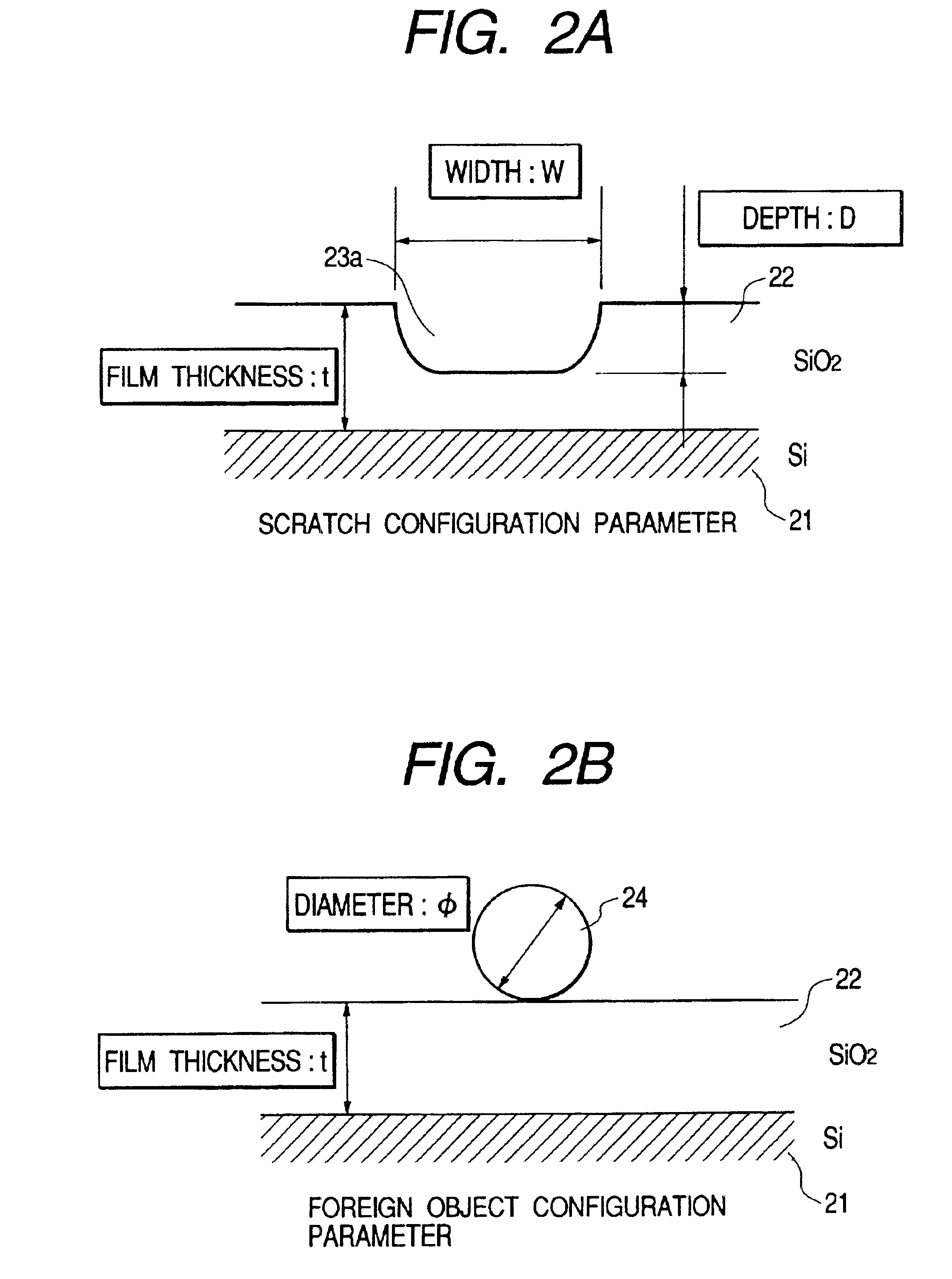
[0102]The discrimination is based on the fact that the scratch 23b having a deep depth D with respect to the width W has a long length inherently. The reason is that the wafer is polished with rotation in CMP process and the deep scratch will not have a short length differently from the nick having a local deep concave. the present invention is based on the above-mentioned certainty, a linear long defect is further classified as the large scratch 23b out of defects recognized as the foreign object 24 in step S64 shown in FIG. 6. At that time, the defect is classified based on the principle shown in FIG. 13A and FIG. 13B. When a light flux 12 is irradiated from the normal line direction onto a large scratch 23b with linear pattern as shown in FIG. 13B, the diffracted light exhibits a distribution having very strong directionality in the right angle direction of the linear pattern 23b. FIG. 13A shows a case in which a light flux 11 is irradiated with inclination from the normal line d...

fourth embodiment

[0110]Next, the fourth embodiment used to further classify the defect 23a that has been discriminated as the scratch by means of two directional illuminations according to configuration will be described in detail hereinafter with reference to FIG. 18 to FIG. 20B. CMP process involves not only the mechanical polishing but also chemical polishing such as etching simultaneously. Therefore, CMP is called as chemical mechanical polishing. Usually, the mechanical polishing action is predominant in the oxide film polishing process, and a typical scratch 23a is a continuous flaw 23aa comprising small linear scratches, each of which is crescent described as tire mark in FIG. 18. On the other hand, when the chemical polishing action is predominant, the V-shaped flaw 23ab having the circular plane cross section described as dimple mark in FIG. 18 is formed often. Furthermore, when a polishing pad that has been used for long time and has become hard is used, crowded small scratches 23ac that i...


PUM


Abstract

The invention provides a surface inspection apparatus and a method for inspecting the surface of a sample that are capable of inspecting discriminatingly between the scratch of various configuration and the adhered foreign object that occur on the surface of a work target when the work target (for example, an insulating film on a semiconductor substrate) is subjected to polishing process such as CMP or grinding process in semiconductor manufacturing process or magnetic head manufacturing process. In the invention, the scratch and foreign object that occur on the polished or ground surface of the sample is epi-illuminated and slant-illuminated by use of approximately same light flux, the difference between the scattered light intensity emitted from the shallow scratch and that from the foreign object when epi-illumination is applied and slant illumination is applied to thereby discriminate between the shallow scratch and the foreign object, and the directionality of the scattered light when the epi-illumination is applied and the slant illumination is applied is detected to thereby discriminate between the linear scratch and the foreign object.

Description

BACKGROUND OF THE INVENTION[0001]The present invention relates to a surface inspection apparatus and a method thereof for discriminatingly inspecting defects such as scratches and foreign objects that arise in the flattening process in which polishing or grinding working technique is applied in semiconductor manufacturing process or magnetic head manufacturing process.[0002]As for the prior art for discriminatingly inspecting a foreign object that adheres on a semiconductor wafer on which a circuit pattern has been formed from the circuit pattern, Japanese Unexamined Patent Publication No. H3-102248 (prior art 1) and Japanese Unexamined Patent Publication No. H3-102249 (prior art 2) have been known. In detail, a method is described in the prior art 1 and the prior art 2, in which a foreign object on a semiconductor substrate is detected by means of a first photoelectric conversion element with emphasis by use of a slant illumination, and an edge of a circuit pattern that is the back...

Claims


Application Information

Patent Timeline
IPC IPC(8): G01N21/88G01N21/95G01B11/24G01B11/30G01B11/245G01N21/956G06T1/00H01L21/66
CPCG01N21/474G01N21/94G01N21/9501G01N21/88G01N2021/8825G01N2021/8854G01N21/9503
Inventor ISHIMARU, ICHIRONOGUCHI, MINORIMORIYAMA, ICHIROTANABE, YOSHIKAZUYATSUGAKE, YASUOKENBOU, YUKIOWATANABE, KENJITSUCHIYAMA, HIROFUMI
Owner HITACHI LTD
Why Eureka
Try Eureka