Series terminated CMOS output driver with impedance calibration

a series terminating and output driver technology, applied in the field of line drivers, can solve the problems of additional delay variation and mismatch, inefficient use of available current, and driver structure of fig

Inactive Publication Date: 2005-05-17
AVAGO TECH WIRELESS IP SINGAPORE PTE
View PDF9 Cites 26 Cited by
  • Summary
  • Abstract
  • Description
  • Claims
  • Application Information

AI Technical Summary

Benefits of technology

[0018]The present invention is directed to a series terminated CMOS output driver with impedance c...

Problems solved by technology

There are several drawbacks to the driver structure of FIG.
Even if the logic were to be made similar, the loading for the output of the logic circuits would be different, since typically PMOS transistors are larger than NMOS transistors, and this can cause addit...

Method used


Image

  • Series terminated CMOS output driver with impedance calibration
  • Series terminated CMOS output driver with impedance calibration
  • Series terminated CMOS output driver with impedance calibration

Examples


Embodiment Construction

[0034]Reference will now be made in detail to the embodiments of the present invention, examples of which are illustrated in the accompanying drawings.

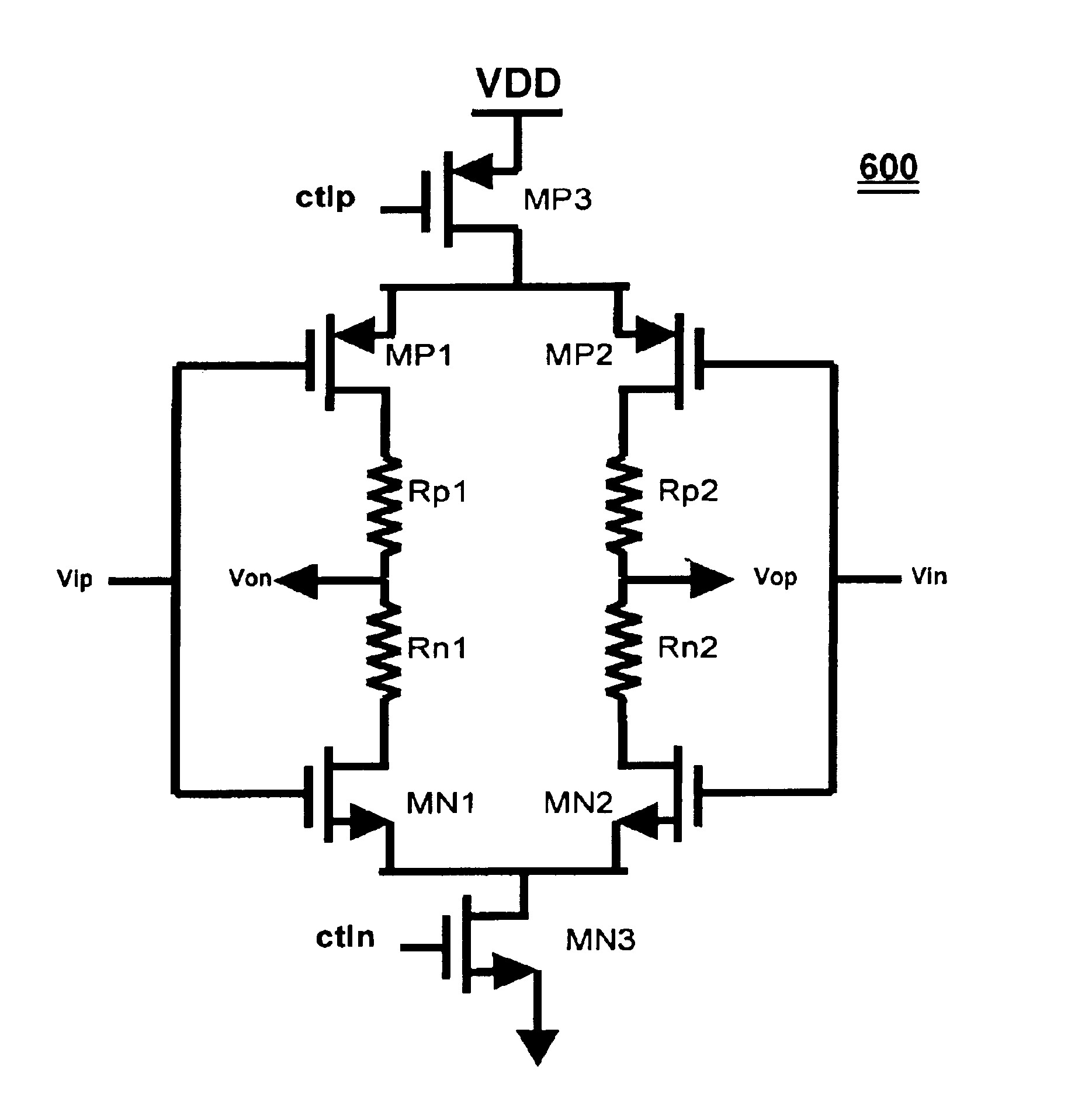
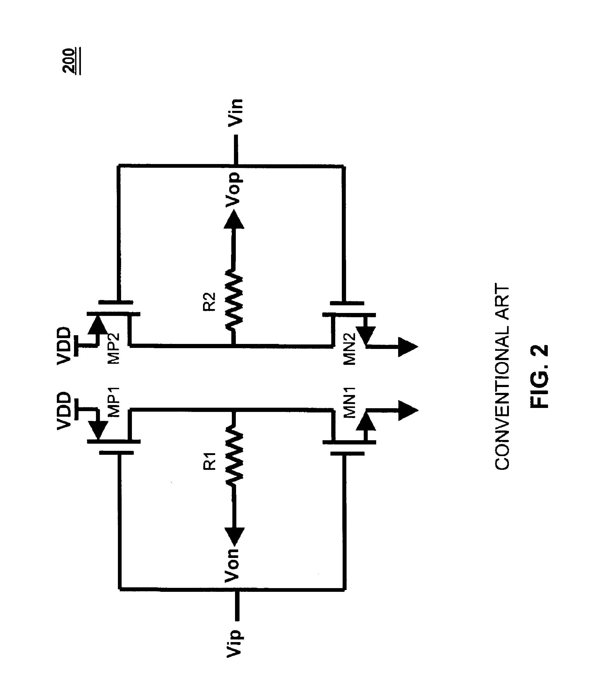
[0035]The proposed invention overcomes the disadvantages outlined for both the driver structure of FIG. 2, the segmented structure of FIG. 4, its associated calibration circuitry of FIG. 5 and the similar scheme described in Gabara et al.

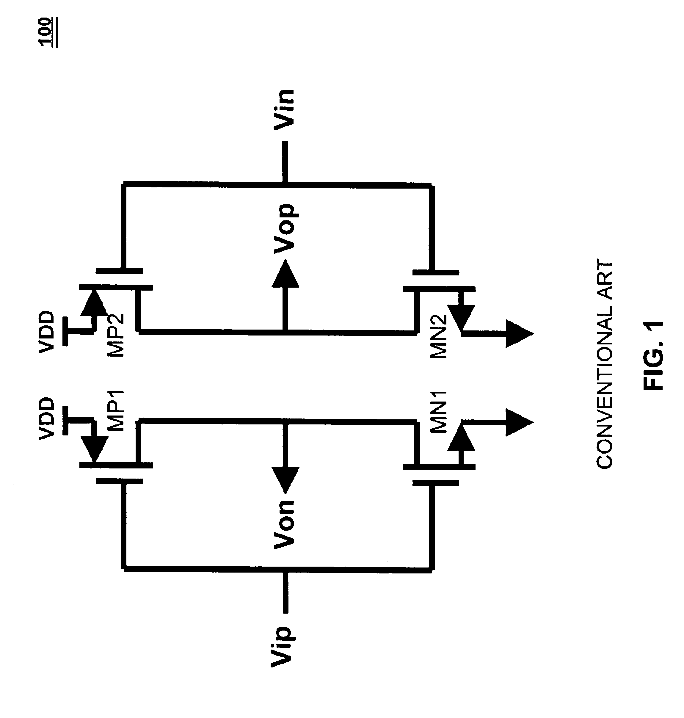
[0036]The output impedance of prior art inverter type drivers as shown in FIG. 1 changes significantly with the output voltage. For the present invention, if the resistors and transistors are sized such that the resistors provide the dominant termination impedance, then the output impedance of the driver will vary insignificantly with respect to the output voltage.

[0037]Conventional inverter drivers share the same signal and control path.

[0038]In the present invention, the signal path and control path are separated, allowing the removal of any control logic in the signal path.

[0039]The transient shoot...


PUM


Abstract

A differential line driver includes a plurality of driver cells. Control logic outputs positive and negative control signals to the driver cells so as to match a combined output impedance of the driver cells at (Vop, Von). Each driver cell includes an input Vip and an input Vin, an output Vop and an output Von, a first PMOS transistor and a first NMOS transistor having gates driven by the input Vip, and a second PMOS transistor and a second NMOS transistor having gates driven by the input Vin. A source of the first PMOS transistor is connected to a source of the second PMOS transistor. A source of the first NMOS transistor is connected to a source of the second NMOS transistor. First and second resistors are connected in series between the first PMOS transistor and the first NMOS transistor, and connected together at Von. Third and fourth resistors are connected in series between the second PMOS transistor and the second NMOS transistor, and connected together at Vop. A first output switch is driven by a corresponding positive control signal and connected between a supply voltage and the sources of the first and second PMOS transistors. A second output switch driven by a corresponding negative control signal and connected between a ground and the sources of the first and second PMOS transistors.

Description

CROSS-REFERENCE TO RELATED APPLICATIONS[0001]This application is a continuation of U.S. patent application No. 10 / 419,886, file on Apr. 22, 2003, entitled SERIES TERMINATED CMOS OUTPUT DRIVER WITH IMPEDANCE CALIBRATION, now U.S. Pat. No. 6,771,097, which is incorporated herein by reference.BACKGROUND OF THE INVENTION[0002]1. Field of the Invention[0003]The present invention relates to line drivers, and more particularly, to differential line drivers with impedance that is matched to the line.[0004]2. Description of the Related Art[0005]In high speed signaling systems, drivers with output impedance matched to the line impedance are used. A conventional voltage mode series terminated driver can be realized using an inverter with proper sizing of the NMOS and PMOS transistors to give an output impedance equal to the line impedance, which is typically 50 ohms. A circuit implementation of such a driver 100 in its differential form is shown in FIG. 1.[0006]Referring to FIG. 1, PMOS transi...

Claims


Application Information

Patent Timeline
IPC IPC(8): H03K19/00H04L25/08H04L25/02
CPCH03K19/0005H04L25/0272H04L25/085H04L25/028H04L25/0278
Inventor HO, DAVID SENG POHLEE, WEE TECK
Owner AVAGO TECH WIRELESS IP SINGAPORE PTE
Why Eureka
Try Eureka