Liquid crystal display device having improved seal pattern and method of fabricating the same

a liquid crystal display and seal pattern technology, applied in non-linear optics, instruments, optics, etc., can solve the problems of deteriorating resolution characteristics of lcd devices, light may leak from the panel, and liquid crystal cells cannot adequately perform their functions, so as to achieve improved seal patterns

Inactive Publication Date: 2005-05-17
LG DISPLAY CO LTD
View PDF13 Cites 13 Cited by
  • Summary
  • Abstract
  • Description
  • Claims
  • Application Information

AI Technical Summary

Benefits of technology

[0036]Accordingly, the present invention is directed to a liquid crystal display device having an improved seal pattern and method of fabricating the same that substantially obviate one or more of problems due to limitations and disadvantages of the related art.

Problems solved by technology

Since static electricity can be harmful to the liquid crystal, the non-electric spray method is more widely used than the electric spray method.
If the upper and lower substrates are aligned and attached beyond the aligning margin, light may leak from the panel such that the liquid crystal cell cannot adequately performed its function.
As a result, resolution characteristics of the LCD device are deteriorated.
However, the above-mentioned structure does not provide a required adhesion, and also it does not sufficiently enlarge the seal pattern area that is the contacting area between the seal pattern 2 and the array substrate 23.
Moreover, to obtain a large contacting area, enlarging the width of the seal pattern 2 is not good enough because of an aperture ratio.

Method used


Image

  • Liquid crystal display device having improved seal pattern and method of fabricating the same
  • Liquid crystal display device having improved seal pattern and method of fabricating the same
  • Liquid crystal display device having improved seal pattern and method of fabricating the same

Examples


first embodiment

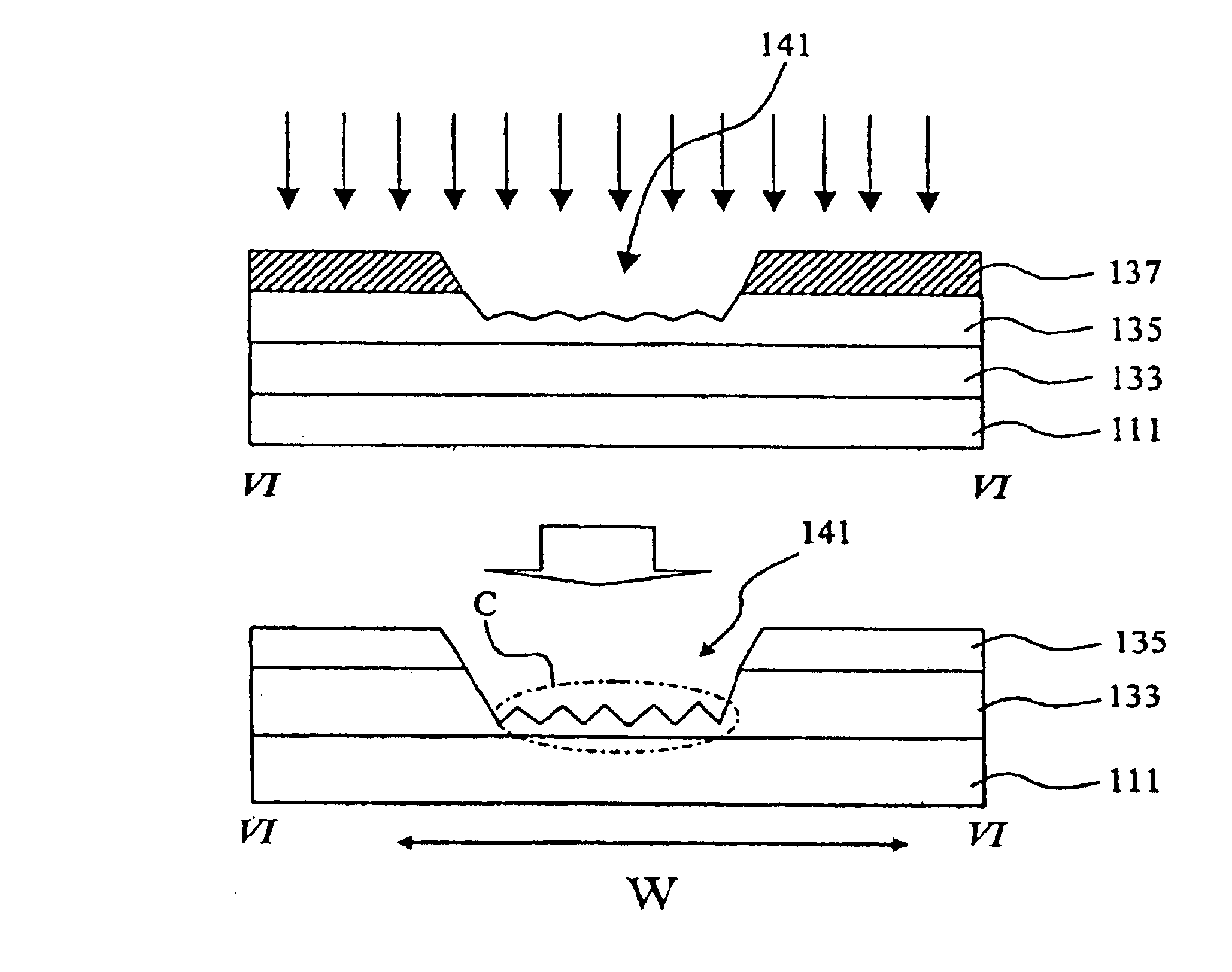
[0059]FIGS. 6A to 6C are cross-sectional views taken along the line VI—VI of FIG. 4 illustrating fabricating processes for a seal pattern according to the present invention.

[0060]FIG. 6A illustrates a photoresist process for forming an etching hole in a seal pattern area of an array substrate. As shown in the drawing, a gate insulation layer 133 and a passivation layer 135 are stacked on a substrate 111. Here, the gate insulation layer 133 is formed of an inorganic material while the passivation layer 135 is made of an organic material. The seal pattern area for a seal pattern is determined in the edges of the stacked structure of the array substrate. In order to form an etching hole, a photoresist layer 137 is formed on the entire surface of the passivation layer 135. A light exposure process is then performed using a mask 139.

[0061]In this process, the mask 139 has a plurality of slits 140 corresponding to the seal pattern area such that the light “A” passing the slits 140 is diff...

second embodiment

[0069]FIGS. 7A to 7C are cross-sectional views taken along the line VI—VI of FIG. 4 illustrating fabricating processes for a seal pattern according to the present invention.

[0070]FIG. 7A illustrates a photoresist process for patterning a passivation layer and a gate insulation layer in the seal pattern area of the array substrate. As shown in the drawing, the gate insulation layer 233 and the passivation layer 235 are stacked on a substrate 221. Here, the gate insulation layer 233 is an inorganic material and the passivation layer 235 is an organic material. A photoresist layer 237 is formed on the passivation layer 235.

[0071]After performing a light exposure process using a mask (not shown), some portions of the photoresist layer 237 are stripped off in order to form projecting portions “f1” and indented portions “f2”. The indented portions “f2” expose the surface of the passivation layer 235. The patterned portion of the photoresist layer 237 is as wide as the width “W” of the sea...

third embodiment

[0077]In general, the array substrate includes a switching element, a gate, and data lines, which are formed thereon. The sequential configuration order for forming the gate and data lines depends on the TFT type, as described before. In a third embodiment, an inverted staggered type TFT is elected as an example. Thus, detailed explanation will be focused on the inverted staggered type TFT.

[0078]According to the inverted staggered type TFT, as shown in FIG. 5A, the gate lines are initially formed on the substrate. The insulation layer is then formed on the substrate to cover the gate lines. Thereafter, the data lines are formed on the insulation layer. Thus, the data lines are insulated from the gate lines by the insulation layer. Moreover, the passivation layer is formed to cover the data lines.

[0079]FIGS. 8A to 8C and 9A to 9C are cross-sectional views taken along the line VI—VI of FIG. 4 illustrating fabricating processes for a seal pattern according to a third embodiment of the ...


PUM

PropertyMeasurementUnit
areaaaaaaaaaaa
latticeaaaaaaaaaa
adhesionaaaaaaaaaa

Abstract

A liquid crystal display having a substrate includes a plurality of gate lines extended from each gate on the substrate, a gate insulating layer on the substrate including the gate lines, a plurality of data lines arranged to be perpendicular to the gate lines, a passivation layer over the data lines and the gate insulation layer, a plurality of etching holes in the passivation layer and the gate insulating layer, wherein the gate insulating layer within the etching holes has at least one concave and convex portions, and a plurality of seal pattern lines in the etching holes.

Description

[0001]This application claims the benefit of Korean Application No. 2000-26786 filed May 18, 2000, which is hereby incorporated by reference.BACKGROUND OF THE INVENTION[0002]1. Field of the Invention[0003]The present invention relates to a liquid crystal display device, and more particularly, to a liquid crystal display device having an improved seal pattern and method of fabricating the same. Although the present invention is suitable for a wide scope of applications, it is particularly suitable for enhancing adhesion between a sealant and an array substrate, thereby providing high yield.[0004]2. Discussion of the Related Art[0005]Liquid crystal display (LCD) devices having light, thin, low power consumption characteristics have been widely used in office automation (OA) equipment and video units. A typical liquid crystal display (LCD) panel has upper and lower substrates and an interposed liquid crystal layer. The upper substrate, referred to as a color filter substrate, usually i...

Claims


Application Information

Patent Timeline
Patent Type & Authority Patents(United States)
IPC IPC(8): G02F1/13G02F1/1362G02F1/1339G02F1/1333
CPCG02F1/1339G02F1/136227G02F2001/133357G02F1/133357G02F1/136
Inventor BAE, SUNG-SIK
Owner LG DISPLAY CO LTD
Why Eureka
Try Eureka