Magnetic random access memory (MRAM) for spontaneous hall effect and method of writing and reading data using the MRAM

a random access memory and spontaneous hall effect technology, applied in the field of random access memory, can solve the problems of increased noise, shortening the operating time of the cell, and degrading so as to improve the thermal security of the cell, increase the coercivity, and high integration

Inactive Publication Date: 2005-05-17
SAMSUNG ELECTRONICS CO LTD
View PDF3 Cites 10 Cited by
  • Summary
  • Abstract
  • Description
  • Claims
  • Application Information

AI Technical Summary

Benefits of technology

[0024]An MRAM according to an embodiment of the present invention, increases the coercivity caused by high integration and improves the thermal security of a cell. The MRAM is able to operate at an ultrahigh speed because of a small cell resistance. In addition, since the MRAM may be simply manufactured using existing semiconductor manufacturing processes, the manufacturing costs are reduced. Furthermore, since the MRAM writes or reads data using the fact that a spontaneous Hall voltage greatly differs according to the magnetization state of a memory layer, an MRAM of the present invention provides a high data sensing margin.

Problems solved by technology

However, when the TMR memory is downsized, an operating time thereof is lengthened and noise is increased, since the TMR memory has a significant amount of resistance, for example, about 106 Ω-μm2.
In such conventional MRAMs, when a cell size is reduced to a size of sub-microns or less, coercivity increases, and the thermal security of a cell degrades.
These characteristics prevent a high level of integration.

Method used


Image

  • Magnetic random access memory (MRAM) for spontaneous hall effect and method of writing and reading data using the MRAM
  • Magnetic random access memory (MRAM) for spontaneous hall effect and method of writing and reading data using the MRAM
  • Magnetic random access memory (MRAM) for spontaneous hall effect and method of writing and reading data using the MRAM

Examples


Embodiment Construction

[0029]Korean Patent Application No. 2002-35141, filed on Jun. 22, 2002, and entitled: “Magnetic Random Access Memory (RAM) Using Thermo-Magnetic Spontaneous Hall Effect and Method of Writing and Reading Data Using the Magnetic RAM,” is incorporated by reference herein in its entirety.

[0030]The present invention will now be described more fully hereinafter with reference to the accompanying drawings, in which preferred embodiments of the invention are shown. The invention may, however, be embodied in different forms and should not be construed as limited to the embodiments set forth herein. Rather, these embodiments are provided so that this disclosure will be thorough and complete, and will fully convey the scope of the invention to those skilled in the art. In the drawings, the thickness of layers and regions are exaggerated for clarity. Like numbers refer to like elements throughout.

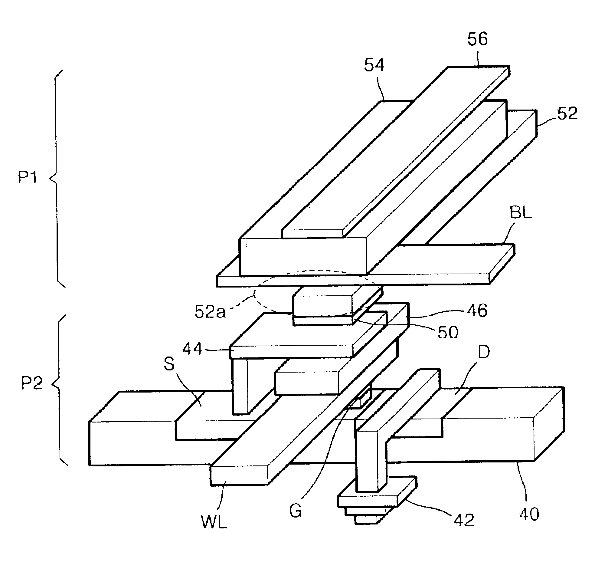
[0031]A magnetic random access memory (MRAM) according to an embodiment of the present invention is...


PUM


Abstract

A magnetic RAM (MRAM) using a thermo-magnetic spontaneous Hall effect includes a MOS transistor formed on a substrate; a heating layer formed above the MOS transistor and connected to a source region of the MOS transistor; a memory layer having a data write area to which data is written, the data write area being formed on the heating means; a bit line formed on the data write area; an upper insulating film formed on the bit line and the memory layer; and a write line formed on the upper insulating film so that a magnetic field necessary for writing data is generated in at least the data write area of the memory layer. The MRAM writes or reads data using the fact that a spontaneous Hall voltage greatly differs according to the magnetization state of a memory layer, thereby providing the device a high data sensing margin.

Description

BACKGROUND OF THE INVENTION[0001]1. Field of the Invention[0002]The present invention relates to the field of magnetic random access memory (MRAM) and methods of writing and reading data using the MRAM. More particularly, the present invention relates to an MRAM using a thermo-magnetic spontaneous Hall effect and a method of writing and reading data using the MRAM.[0003]2. Description of the Related Art[0004]Giant MagnetoResistance (GMR) is derived by a variation in the resistance of a thin film depending on whether two adjacent magnetic layers are magnetized in parallel or counter-parallel directions when electrons pass through the two magnetic layers. GMR may be described with reference to spin-dependent scattering. Even when an insulating film, such as an aluminum oxide film (Al2O3), as opposed to a metallic film, is interposed between the two magnetic layers, spin-dependent scattering occurs. Spin-dependent scattering is referred to as Tunneling MagnetoResistance (TMR).[0005]Con...

Claims


Application Information

Patent Timeline
Patent Type & Authority Patents(United States)
IPC IPC(8): G11C11/18H01L27/105G11C11/15H01L21/8246H01L43/06
CPCG11C11/18G11C11/1675G11C11/15
Inventor KIM, TAE-WANKIM, KEE-WONPARK, WAN-JUNSONG, I-HUNPARK, SANG-JIN
Owner SAMSUNG ELECTRONICS CO LTD
Why Eureka
Try Eureka