System and method for VLSI visualization

a visualization system and visualization technology, applied in the field of visualization, can solve the problems of increasing complexity and complexity of integrated circuits, increasing the difficulty of ic designers to complete a design, and increasing the difficulty of design verification and testing,

Inactive Publication Date: 2005-05-17
GLOBALFOUNDRIES INC
View PDF23 Cites 44 Cited by
  • Summary
  • Abstract
  • Description
  • Claims
  • Application Information

AI Technical Summary

Benefits of technology

[0006]It is an object of this invention to provide a system and method to visualize the simulated internal functioning of ICs for effective design evaluation, design of test, and comparison to the measured internal functioning of ICs as measured using techniques such as the newly available photon emission measurement also known as PICA. An output of the PICA system is a visual representation of transistor switching events, in the form of a slow motion video. The present invention is related to visualization of simulated IC activity. One form of activity further described in the preferred embodiment is the simulated version of the PICA slow motion “movie”. This has multiple uses, including i) predicting and thereby preparing test and analysis approaches for PICA measurement, ii) learning through visual study of the switching behavior aligned to the physical layout or optical microscope image, iii) flagging of improper behavior such as incorrect logical operation occurring during certain ranges of simulation conditions, and iv) comparison of the visualizations between simulation and measured data sets.

Problems solved by technology

As integrated circuits (IC) become increasingly dense and complex, all aspects of design, including custom and synthesized design, design verification and testing are becoming more and more difficult.
The immensity of the data and the complex interrelationships among the various aspects of design including the design data, technology, and test, make it extremely difficult for IC designers to complete a design with confidence that it will function at the intended performance, and be manufacturable and reliable.
Thinning of the chip further increases the complexity of preparation of test.

Method used


Image

  • System and method for VLSI visualization
  • System and method for VLSI visualization
  • System and method for VLSI visualization

Examples


Embodiment Construction

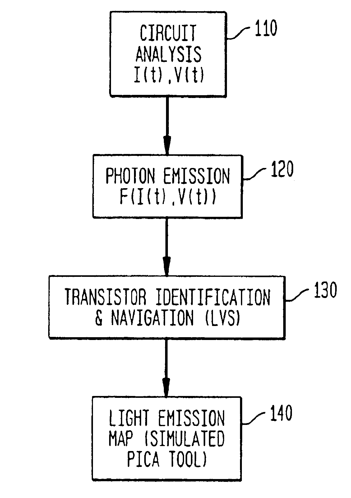
[0018]The preferred embodiment provides a system, structures, and method by which visualization of the simulated circuit behaviors and properties is performed within an IC CAD viewer. These visualizations are viewable within the IC viewer along with the regular device views and measured IC data, verification traces, logical data, and test data. In the case of electrical simulation, currents simulated at nets can be computed to form PICA representations, time varying power maps at the individual transistor and net level, noise, and electromigration maps, to name a few types of visualizations. The novelty of electrical simulation visualization is the viewing of complex circuit activity in an intuitive fashion, down to the individual device level. This can be related to measured circuit activity at the device level by methods such as PICA. As mentioned in the background, there are situations where simulated PICA is more accessible than the physically measured PICA for the analysis of d...


PUM


Abstract

A method and system for visualizing circuit operation. In the method device activity is obtained based on one or more of measured or simulated activity. The device activity is expressed in a representation, and the expressed activity is represented in a visual form. One suitable form of activity is the simulated version of the PICA slow motion movie. The invention may apply to other simulated design data vies as well, such as switch level simulation, current density simulation, and power density simulation.

Description

FIELD OF THE INVENTION[0001]The invention relates to visualization as an aid to the design, verification, and test of integrated circuits.BACKGROUND OF THE INVENTION[0002]As integrated circuits (IC) become increasingly dense and complex, all aspects of design, including custom and synthesized design, design verification and testing are becoming more and more difficult. The immensity of the data and the complex interrelationships among the various aspects of design including the design data, technology, and test, make it extremely difficult for IC designers to complete a design with confidence that it will function at the intended performance, and be manufacturable and reliable. Design aids that enable the visualization of circuit functionality, simulated under various operating conditions, process conditions, and electrical input conditions, that are interactive and cross-probeable with the device and circuit elements of the design views would greatly enhance the ability to create r...

Claims


Application Information

Patent Timeline
Patent Type & Authority Patents(United States)
IPC IPC(8): G06F17/50H01L21/76H01L21/70
CPCG06F17/5022G06F30/33
Inventor KNEBEL, DANIEL R.LAVIN, MARK A.MORENO, JAMIEPOLONSKY, STANISLAVSANDA, PIA N.VOLDMAN, STEVEN H.
Owner GLOBALFOUNDRIES INC
Why Eureka
Try Eureka