Strain-engineered direct-gap Ge/SnxGe1-x heterodiode and multi-quantum-well photodetectors, laser, emitters and modulators grown on SnySizGe1-y-z-buffered silicon

a technology of snxge1-y-z-buffered silicon and heterodiode, which is applied in the direction of semiconductor devices, lasers, semiconductor devices, etc., can solve the problems of high cost, low quality, and hybrid integration approach

Inactive Publication Date: 2005-05-24
THE GOVERNMENT OF THE US SEC THE AIR FORCE
View PDF4 Cites 73 Cited by
  • Summary
  • Abstract
  • Description
  • Claims
  • Application Information

AI Technical Summary

Problems solved by technology

This is a deficiency because elemental Ge is easy to deposit in a heteroepitaxial structure, and because recent research shows that an MQW having tensile Ge barriers and compressive GeSn wells in alternating layers with Type I band alignment is an excellent means for obtaining direct-gap wells.
Free-space devices, described here, are omitted from the prior patent, which is another deficiency because free-space devices such as normal-incidence photodetectors and surface-emitting lasers, are important.
There is prior photonic art on Ill-V alloy structures hybrid-integrated on silicon, but this hybrid integration approach is deficient because the Si-to-III-V lattice mismatch creates difficulty and complexity in processing, tends to make the resulting structures costly and lower in quality.

Method used


Image

  • Strain-engineered direct-gap Ge/SnxGe1-x heterodiode and multi-quantum-well photodetectors, laser, emitters and modulators grown on SnySizGe1-y-z-buffered silicon
  • Strain-engineered direct-gap Ge/SnxGe1-x heterodiode and multi-quantum-well photodetectors, laser, emitters and modulators grown on SnySizGe1-y-z-buffered silicon
  • Strain-engineered direct-gap Ge/SnxGe1-x heterodiode and multi-quantum-well photodetectors, laser, emitters and modulators grown on SnySizGe1-y-z-buffered silicon

Examples


Embodiment Construction

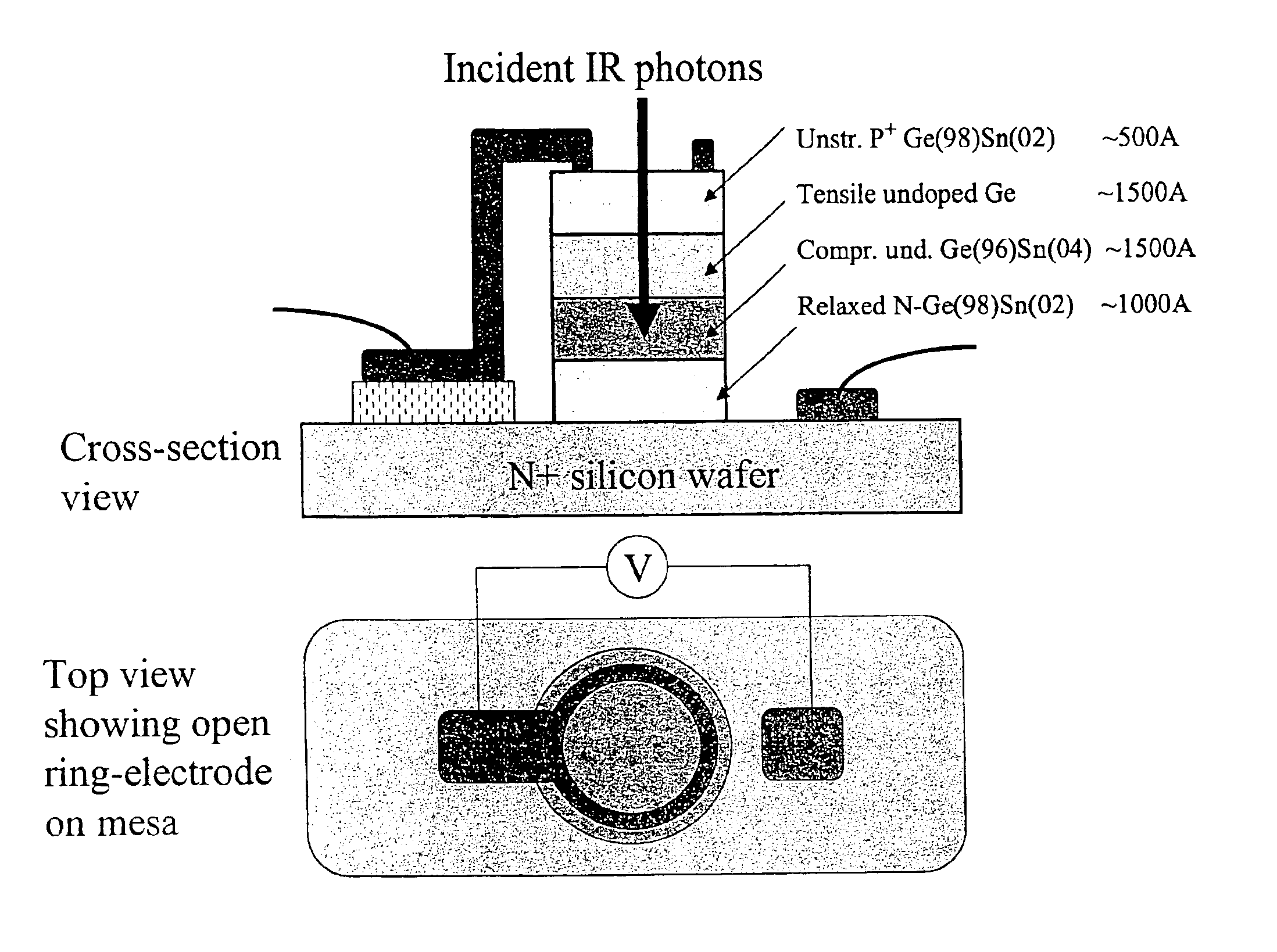
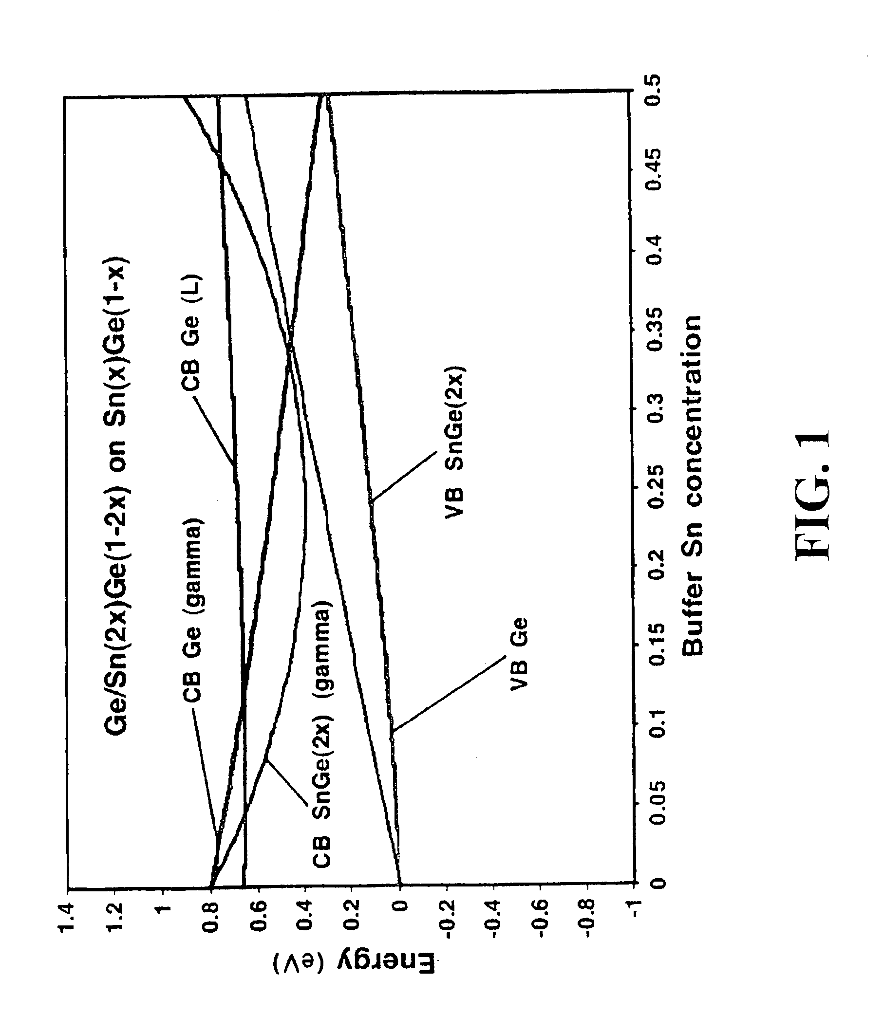
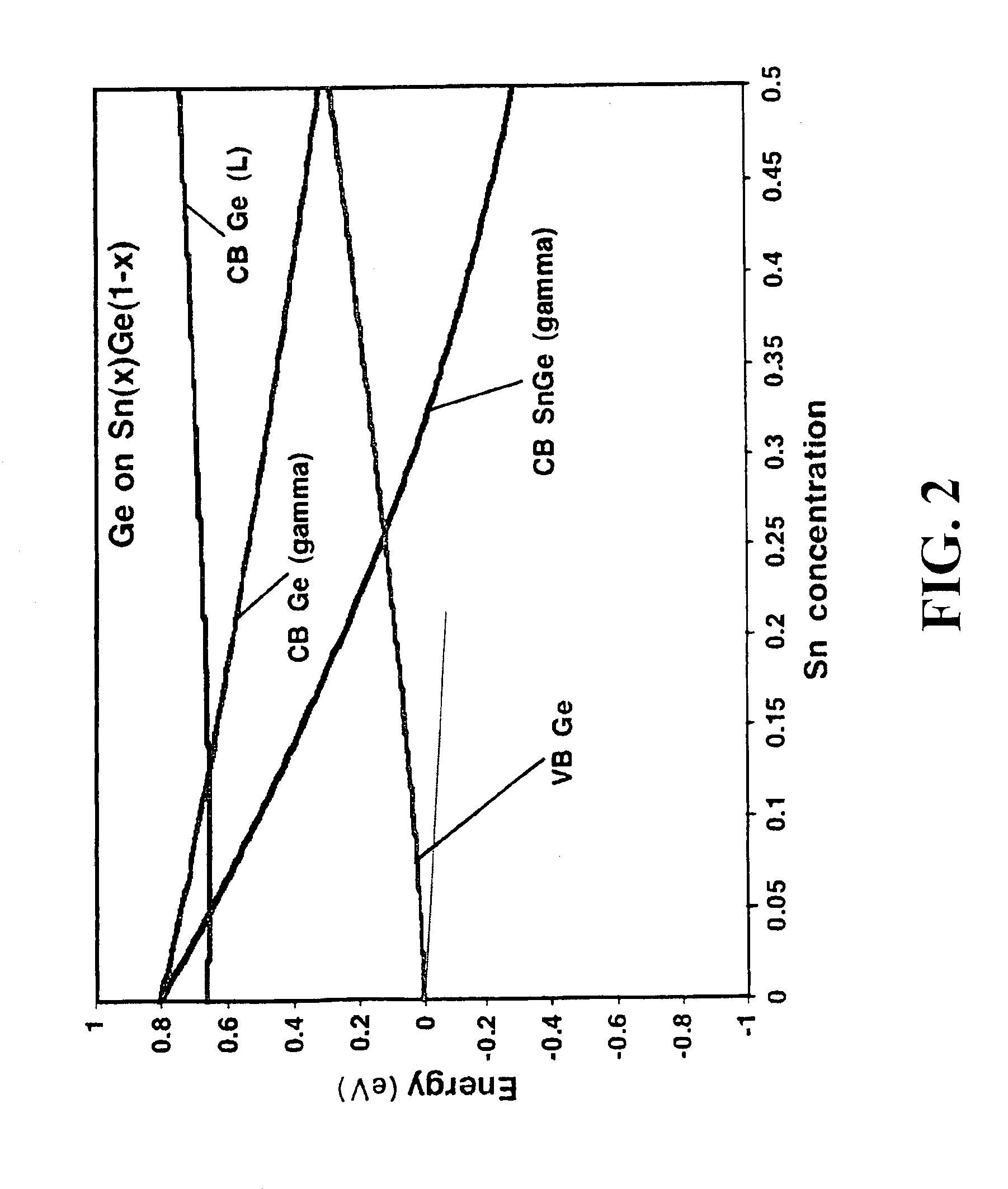
[0014]We describe interband embodiments first, then intersubband devices. We have identified three strained-layer direct-gap structures that are useful for band-to-band photodetection as well as lasing, emission, amplification, and modulation in the near-infrared and middle-infrared regions: (A) strain-compensated Type I MQW of tensile-strained Ge barriers, compressively-strained Ge1-2xSn2x quantum wells, grown upon a relaxed buffer of Ge1-xSnx upon silicon, wherein electrons and holes are confined in Ge1-2xSn2x; (B) an unsymmetrically strained Type-II system of tensile Ge and unstrained Ge1-xSnx grown on relaxed Ge1-xSnx upon silicon, with holes confined in Ge and electrons in Ge1-xSnx; (C) an unsymmetrically strained Type-I system with tensile Ge wells, compressive Ge1-xSnx barriers, grown upon relaxed SiySnxGe1-x-y upon silicon, with electrons and holes in Ge. FIGS. 1, 2, and 3 show the results of our first-principles band-offset calculations. Plotted in the figures are the highe...


PUM


Abstract

This invention teaches two new families of Si-based Ge / SnxGe1-x heterodiode and multiple quantum well (MQW) photonic devices: (1) band-to-band photodetectors, lasers, emitters, amplifiers and modulators for the 1.5 to 12 μm wavelength range; (2) intersubband photodetectors, lasers, emitters and modulators for 12 to 100 μm operation. The bipolar band-to-band devices have applications within the 1.5-2.2, 3-5 and 8-to-12 μm bands. The unipolar intersubband group has longwave infrared and terahertz applications. All strained-layer devices are grown a relaxed SnySizGe1-y-z buffer layer—a virtual substrate (VS) grown directly upon a silicon wafer by unique LT UHV-CVD. The VS provides a low-defect atomic template for subsequent heteroepitaxy and is an essential enabling technique for engineering tensile and compressive strain within the Ge / SnxGe1-x MQW by selecting the VS lattice parameter to be approx midway between the layer lattices.

Description

STATEMENT OF GOVERNMENT INTEREST[0001]The invention described herein may be manufactured and used by or for the Government for governmental purposes without the payment of any royalty thereon.BACKGROUND OF INVENTION[0002]This invention relates generally to the field of active, efficient, silicon-based photonic devices and photonic integrated circuits that are capable of monolithic integration with Si and SiGe electronics. The present invention does not include group III-V and II-VI photonic structures that are hybrid integrated onto silicon; instead, the present invention teaches an “all-group-IV” solution to the problem of active Si-based photonics in which the active strained-layer region consists of binary and / or ternary group IV alloy layers and / or Ge.[0003]The Si-based photonic components and circuits in this invention are valuable for guided-wave and free-space applications. In the guided-wave case, the active devices taught here can merge with undoped silicon waveguides made ...

Claims


Application Information

Patent Timeline
Patent Type & Authority Patents(United States)
IPC IPC(8): H01L31/0264H01L31/0328
CPCB82Y20/00H01L29/155H01L31/035254H01L33/12H01L31/105H01S5/3427H01L33/34
Inventor SOREF, RICHARD A.MENENDEZ, JOSEKOUVETAKIS, JOHN
Owner THE GOVERNMENT OF THE US SEC THE AIR FORCE
Why Eureka
Try Eureka