Optical coupling device

a coupling device and optical technology, applied in the field of optical coupling devices, can solve the problems of affecting reducing the performance of the element, and generating heat from the power consumed for its own operation, so as to improve the safety, improve the efficiency of energy consumption, and simplify the arrangement

Inactive Publication Date: 2005-05-24
SHARP KK
View PDF7 Cites 6 Cited by
  • Summary
  • Abstract
  • Description
  • Claims
  • Application Information

AI Technical Summary

Benefits of technology

[0010]An object of the present invention is to provide an optical coupling device which can realize compulsive cooling, temperature detection, and effective use of en

Problems solved by technology

However, this triac output solid state relay has an inadequacy such that power consumed for its own operation generates heat, and the raised temperature decreases performance of the element.
Further, the generated heat of the load driving semiconductor element also gives thermal stress to the light emitter and the photoreceptor, which affects aged degradation of the elements.
However, the ideas used for the thermal design of a conventional optical coupling device is nearly pushed to the limit, and it greatly interferes downsizing of the

Method used


Image

  • Optical coupling device
  • Optical coupling device
  • Optical coupling device

Examples


example 1

[0033]The following will explain an optical coupling device according to Example 1 of the present invention with reference to a drawing.

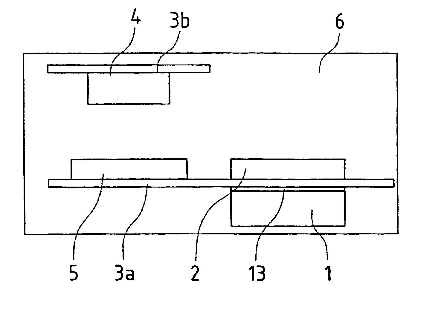
[0034]FIG. 1 is an explanatory view showing an optical coupling device according to Example 1 of the present invention.

[0035]The optical coupling device has an arrangement such that a thermoelectric conversion element 1 is provided on the rear surface (lower surface in FIG. 1) of an output lead frame 3a, which is opposite to a surface having a load driving semiconductor element (for example, a triac) 2.

[0036]The optical coupling device is equipped with the output lead frame 3a and an input lead frame 3b, which are opposed. The output lead frame 3a has a photoreceptor 5 and the load driving semiconductor element 2 on the surface opposing the input lead frame 3b. Further, the thermoelectric conversion element 1 is provided on the other surface of the output lead frame 3a. The thermoelectric conversion element 1 is provided opposite to the load driving...

example 2

[0040]The following will explain an optical coupling device according to Example 2 of the present invention with reference to a drawing.

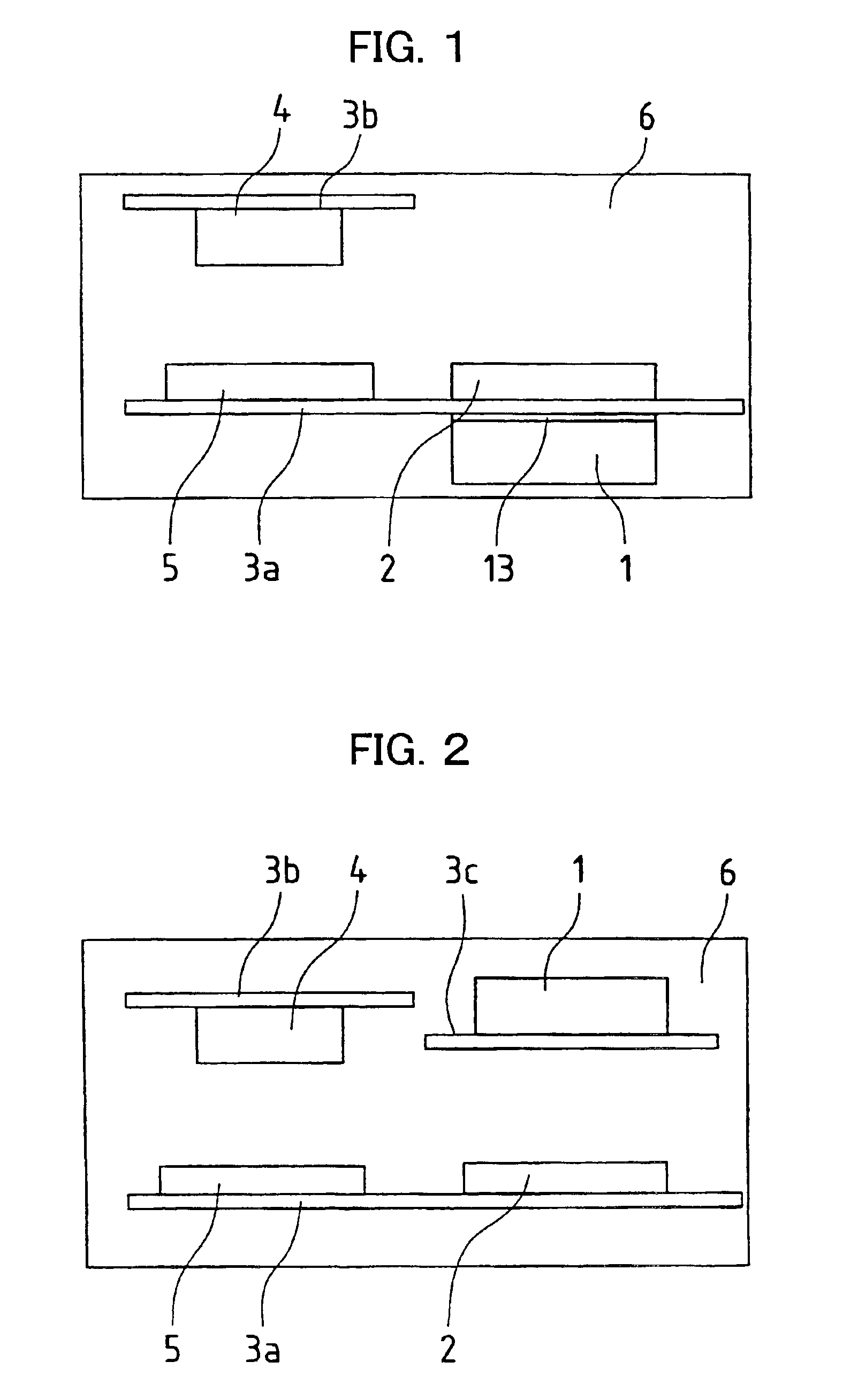
[0041]FIG. 2 is an explanatory view showing an optical coupling device according to Example 2 of the present invention.

[0042]This optical coupling device has substantially the same arrangement as that of Example 1 except for the thermoelectric conversion element 1, which is provided on a thermoelectric conversion element lead frame 3c electrically insulated from the output lead frame 3a having the load driving semiconductor element 2. The thermoelectric conversion element 1 is provided on the upper surface of the thermoelectric conversion element lead frame 3c by being opposite to the load driving semiconductor element 2.

[0043]Namely, the thermoelectric conversion element lead frame 3c is provided opposing the output lead frame 3a. The thermoelectric conversion element 1 is provided on the surface of the thermoelectric conversion element lead frame ...

example 3

[0046]The following will explain an optical coupling device according to Example 3 of the present invention with reference to a drawing.

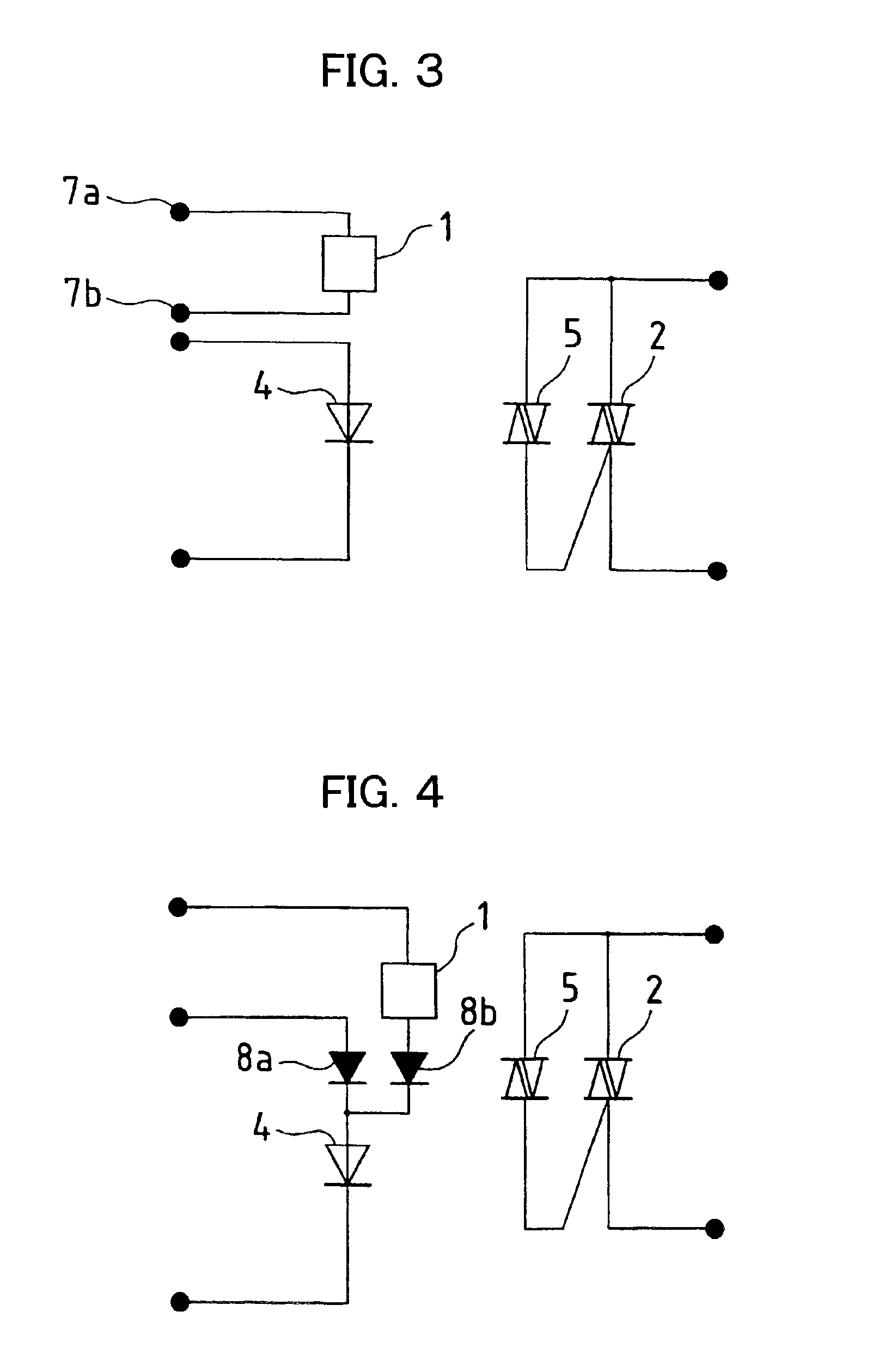
[0047]FIG. 3 is an explanatory view showing an optical coupling device according to Example 3 of the present invention.

[0048]In this optical coupling device, voltage applying means (an input terminal 7a connected to an input section of the thermoelectric conversion element 1, and an output terminal 7b connected to an output section of the thermoelectric conversion element 1) is provided in addition to the arrangement of Example 1 or Example 2 so as to compulsively drop the temperature in the package by using the Peltier effect.

[0049]For example, as shown in FIG. 3, by providing the input terminal 7a and the output terminal 7b connected to the thermoelectric conversion element 1 in the package of the optical coupling device, it is possible to compulsively apply voltage to the thermoelectric conversion element 1. The application of voltage cools one s...


PUM


Abstract

An optical coupling device includes: a light emitter provided on an input lead frame; a photoreceptor provided on an output lead frame; a load driving semiconductor element provided on a front surface of the output lead frame, and connected to the photoreceptor via the output lead frame; and a sealing resin section as a package for protecting the light emitter, the photoreceptor and the load driving semiconductor element, wherein a thermoelectric conversion element is provided in the package.

Description

BACKGROUND OF THE INVENTION[0001]Field of the Invention[0002]The present invention relates to an optical coupling device, which is made of a unified light emitter and photoreceptor by being optically coupled, and in particular to an optical coupling device further including a load driving semiconductor element in the same package, such as a solid state relay.DESCRIPTION OF THE RELATED ART[0003]An example of a conventional optical coupling device may be a solid state relay, which includes a light emitter, a photoreceptor, and a load driving semiconductor element, which are sealed with resin and included in a single package. A solid state relay using a triac as the load driving semiconductor element (hereinafter also referred to as a triac output solid state relay) can be described as an example of the solid state relay.[0004]As shown in FIG. 10, the triac output solid state relay includes a light emitter for converting an electronic signal into light (generally, gallium arsenide LED ...

Claims


Application Information

Patent Timeline
IPC IPC(8): G02B6/42H01L35/28H01L31/12
CPCG02B6/4295G02B6/4201G02B6/4267G02B6/4271G02B6/4268
Inventor YAMAGUCHI, HIROSHI
Owner SHARP KK
Why Eureka
Try Eureka