Liquid crystal display device

a liquid crystal display and active matrix technology, applied in the direction of identification means, instruments, optics, etc., can solve the problems of unstable off-state, inability to stabilize storage potential, and need for large storage capacitance, and achieve stable visual display, high luminance of backlight, and large storage capacitance stable storage potential

Inactive Publication Date: 2005-05-24
PANASONIC LIQUID CRYSTAL DISPLAY CO LTD +1
View PDF13 Cites 45 Cited by
  • Summary
  • Abstract
  • Description
  • Claims
  • Application Information

AI Technical Summary

Benefits of technology

[0014]Advantages of this invention is enable to solve or improve of one or a plurality of the above-described problems. One advantage realize by either one of this invention is to provide a liquid crystal display device which realizes large storage capacitances stable in storage potential and can realize stable visual display even if the luminance of a backlight is high.
[0015]Another advantage realize by either one of this invention is to provide a TFT liquid crystal display device in which an increase storage capacitances in an IPS type of liquid crystal display device which uses low-temperature polysilicon TFTs as pixel TFTs.
[0016]Another advantage realize by either one of this invention is to provide a TFT liquid crystal display device in which in the case where large storage capacitances are provided, no potential other than pixel electrode potential and common electrode potential is applied to a main optically transmissive portion of liquid crystal, whereby it is possible to provide stable visual display in IPS type of liquid crystal display device.
[0017]Another advantage realize by either one of this invention is to provide a TFT liquid crystal display device in which a reduction in short-circuit fraction defective between the electrodes can be prevented even if large storage capacitances are formed.
[0018]Another advantage realize by either one of this invention is to provide a bright TFT liquid crystal display device in which the aperture ratio can be height ened even if large storage capacitances are formed.

Problems solved by technology

This fact results in the problem that a larger storage capacitance is needed for stabilization of the operation of the TFTs.
However, the present inventors have found out that if a stacked structure made of an insulating film and a semiconductor layer is used as a storage capacitance, the potential difference between a pixel electrode and a counter electrode becomes AC voltage and causes the problem that the semiconductor layer is switched on and off during a storage period and storage potential can not be stabilized.
However, in this method, it has been found out that during the state in which the amount of light from the backlight BL increases and intense light strikes the semiconductor layer, the OFF state becomes unstable and the storage potential of the storage capacitance is affected.
Accordingly, a large capacitance variation occurs in the storage capacitance according to the state of driving, so that storage potential cannot be stabilized.

Method used


Image

  • Liquid crystal display device
  • Liquid crystal display device
  • Liquid crystal display device

Examples


embodiment 1

(Embodiment 1)

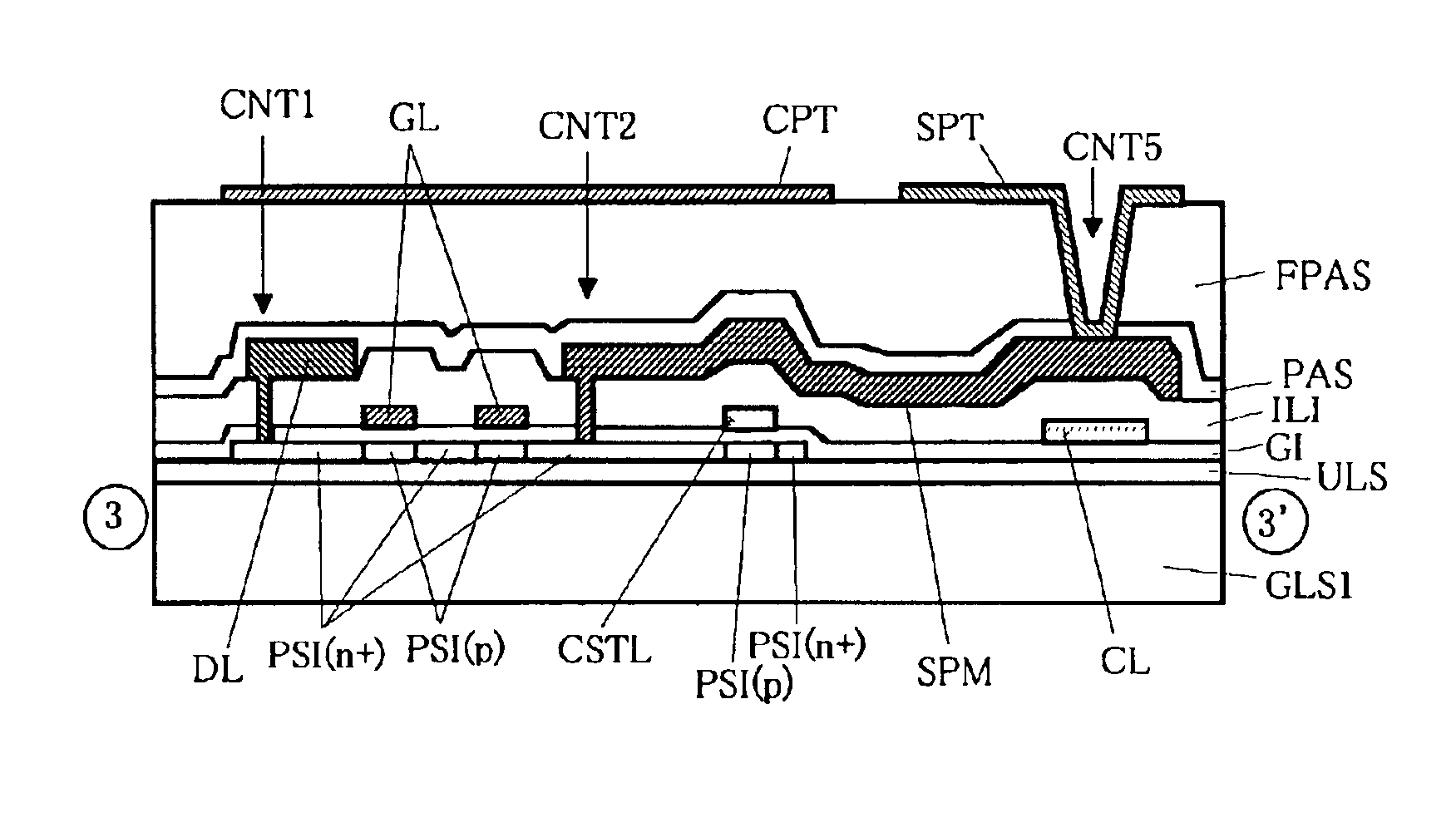
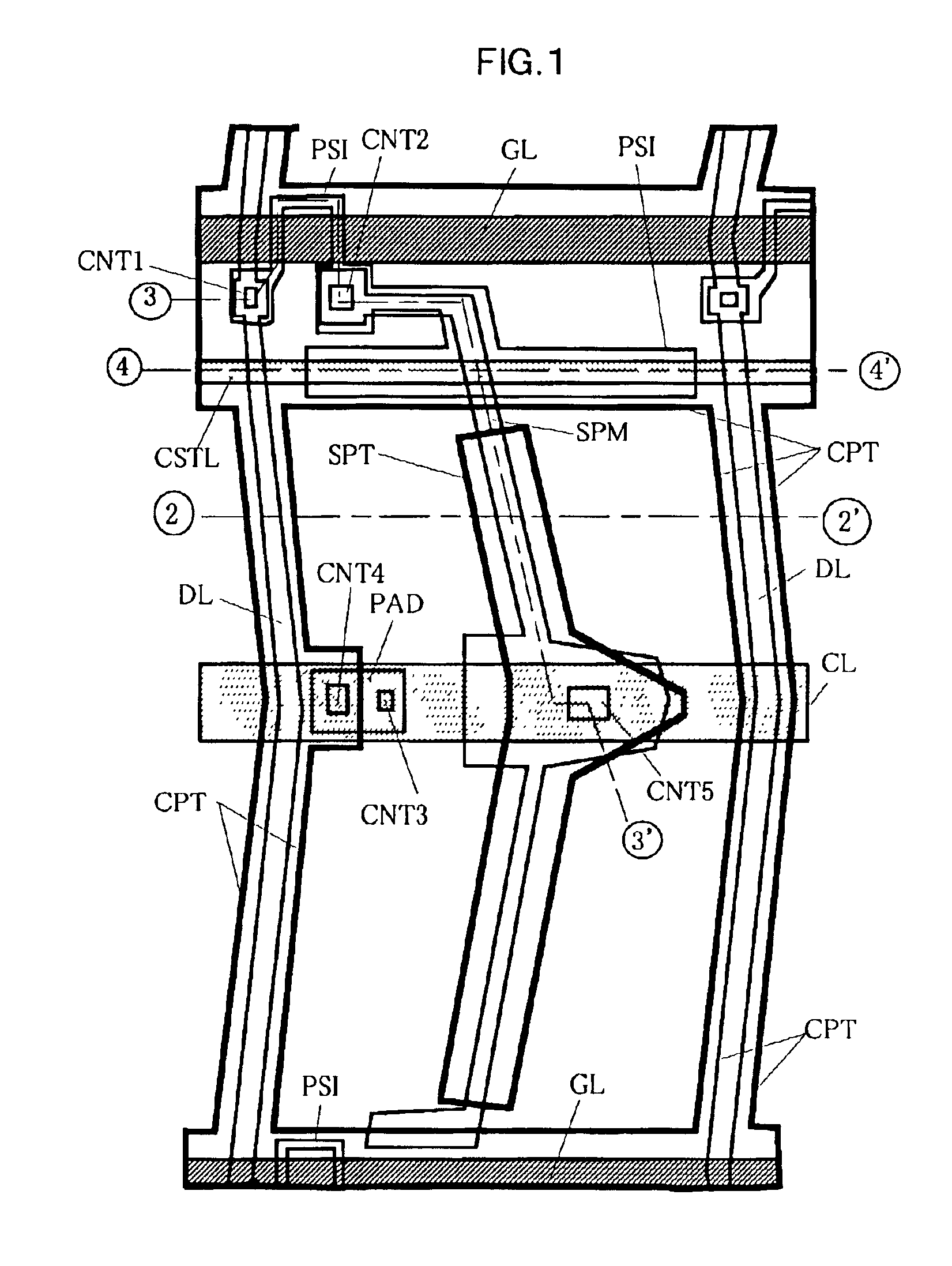
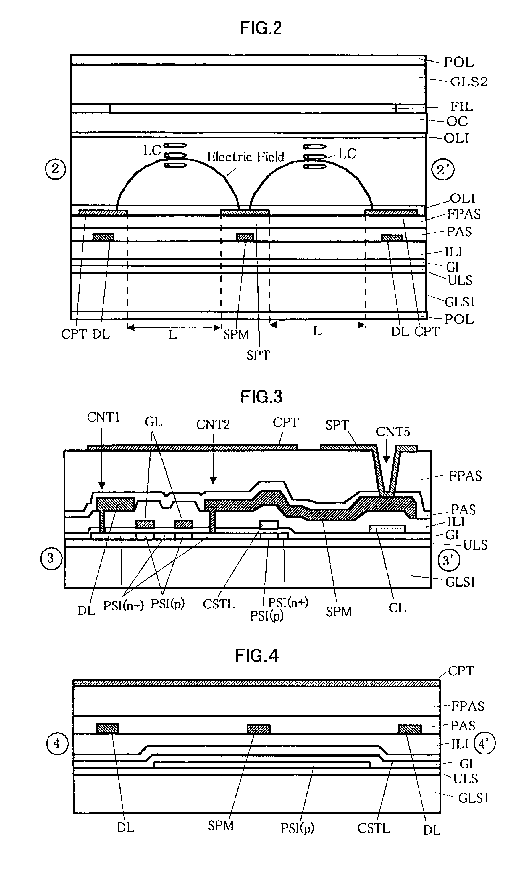
[0080]FIG. 1 is a diagrammatic plan view of a unit pixel of a liquid crystal display device according to Embodiment 1. FIGS. 2, 3 and 4 are diagrammatic cross-sectional views respectively taken along lines 2-2′, 3-3′ and 4-4′ of FIG. 1 (in FIG. 1, these numerals are encircled for ease of understanding).

[0081]In the plane pattern shown in FIG. 1, one pixel is an area surrounded by adjacent gate lines GL and adjacent drain lines DL. A gate line GL (shown in the upper portion of FIG. 1) also functions as a gate electrode of a TFT made of polysilicon PSI at the intersection of the gate line GL and the polysilicon PSI, and supplies a voltage to turn on / off the TFT. A drain line DL (shown in the left portion of FIG. 1) supplies a current to the polysilicon PSI. Specifically, the drain line DL supplies to a liquid crystal capacitance of the one pixel a video voltage (drain voltage) applied at the timing when the gate line GL supplies an ON voltage to the TFT, and the potentia...

embodiment 2

(Embodiment 2)

[0149]FIG. 16 is a diagrammatic plan view of a unit pixel of Embodiment 2, and FIG. 17 shows a cross-sectional structure taken along cutting line 17-17′ of FIG. 16.

[0150]The structure of Embodiment 2 differs from that of Embodiment 1 in that the common electrode line CL shown in FIG. 1 is eliminated which traverses the middle portion of the pixel approximately in parallel with the gate lines GL. Furthermore, in Embodiment 1, the contact holes formed in the insulating film are provided at five locations per pixel, but in Embodiment 2, the number of contact holes per pixel is reduced to three. Accordingly, the number of lines to be formed in the same layer as the gate lines GL is reduced, and therefore, a short-circuit fraction defective is reduced, whereby it is possible to achieve the advantage of an improvement in yield. Furthermore, Embodiment 2 has the advantage that since the number of contact holes is reduced, an open failure (a failure which disables electrical c...

embodiment 3

(Embodiment 3)

[0155]FIG. 18 is a plan view of a unit pixel of Embodiment 3, FIG. 19 shows a cross-sectional structure taken along cutting line 19-19′ of FIG. 18, and FIG. 20 shows a cross-sectional structure taken along cutting line 20-20′ of FIG. 18.

[0156]Although in Embodiments 1 and 2 the storage capacitance line CSTL is disposed adjacent to the gate line GL, in Embodiment 3, the storage capacitance line CSTL is disposed in the middle between the adjacent drain lines DL, i.e., in the position where the common electrode line CL is disposed in Embodiment 1 shown in FIG. 1. Furthermore, this storage capacitance line CSTL is covered with the common electrode CPML and the metal pixel electrode SPM in such a manner that the common electrode CPML and the metal pixel electrode SPM overlap one on top of the other in plan view. Accordingly, it is possible to realize a shield which blocks leak electric fields from the storage capacitance line CSTL while preventing short-circuiting.

[0157]In ...


PUM

PropertyMeasurementUnit
luminanceaaaaaaaaaa
strain pointaaaaaaaaaa
thicknessaaaaaaaaaa

Abstract

In a liquid crystal display device, a capacitance element uses a semiconductor layer as one electrode and is formed between the semiconductor layer and a storage capacitance line with an insulating film interposed therebetween, and a voltage which constantly brings a MOS type transistor into an ON state is applied to the storage capacitance line.

Description

BACKGROUND OF THE INVENTION[0001]1. Field of the Invention[0002]The present invention relates to a liquid crystal display device and, more particularly, to an active matrix type liquid crystal display device of a thin film transistor (TFT) type or the like.[0003]2. Description of the Related Art[0004]Liquid crystal display devices, because of their features such as thin size, light weight and low power consumption, are widely used as display devices for image information and character information in information equipment represented by personal computers, mobile types of information terminals, mobile telephones, and visual equipment such as digital cameras and camera-integrated type VTRs. In recent years, the fusion of personal computers and video digital media has proceeded owing to the appearance of DVDs, the popularization of large capacity media resulting from the rapid evolution of large-capacity magnetic disk drives, and the start of BS digital broadcasting, so that demands fo...

Claims


Application Information

Patent Timeline
Patent Type & Authority Patents(United States)
IPC IPC(8): G02F1/13G02F1/1362G02F1/1343G02F1/1368G02F1/133G02F1/136G09F9/30G09F9/35
CPCG02F1/136213G02F1/134363G02F2202/104G02F1/1368G02F1/136
Inventor OCHIAI, TAKAHIROOKE, RYUTAROIMAYAMA, HIROTAKAONO, KIKUO
Owner PANASONIC LIQUID CRYSTAL DISPLAY CO LTD
Why Eureka
Try Eureka