Method of programming a flash memory through boosting a voltage level of a source line

a source line and voltage level technology, applied in the field of flash memory programming, can solve the problems of difficult to reduce the overall size of the flash memory, and achieve the effect of reducing the chip size occupied by the charge pump circuit and ease of power requirement of the charge pump circui

Inactive Publication Date: 2005-05-24
POWERCHIP SEMICON CORP
View PDF1 Cites 41 Cited by
  • Summary
  • Abstract
  • Description
  • Claims
  • Application Information

AI Technical Summary

Benefits of technology

[0014]It is an advantage of the present invention that a charge pump circuit encounters a smaller loading capacitor when driving a source line. Therefore, the charge pump circuit is merely required to provide a small driving current. Therefore, the power requirement of the charge pump circuit is eased, and the chip size occupied by the charge pump circuit is reduced.
[0015]These and other objectives of the present invention will no doubt become obvious to those of ordinary skill in the art after reading the following detailed description of the preferred embodiment, which is illustrated in the various figures and drawings.

Problems solved by technology

Therefore, it is difficult to reduce the overall size of the flash memory 10 owing to the implemented charge pump circuit.

Method used


Image

  • Method of programming a flash memory through boosting a voltage level of a source line
  • Method of programming a flash memory through boosting a voltage level of a source line
  • Method of programming a flash memory through boosting a voltage level of a source line

Examples


Embodiment Construction

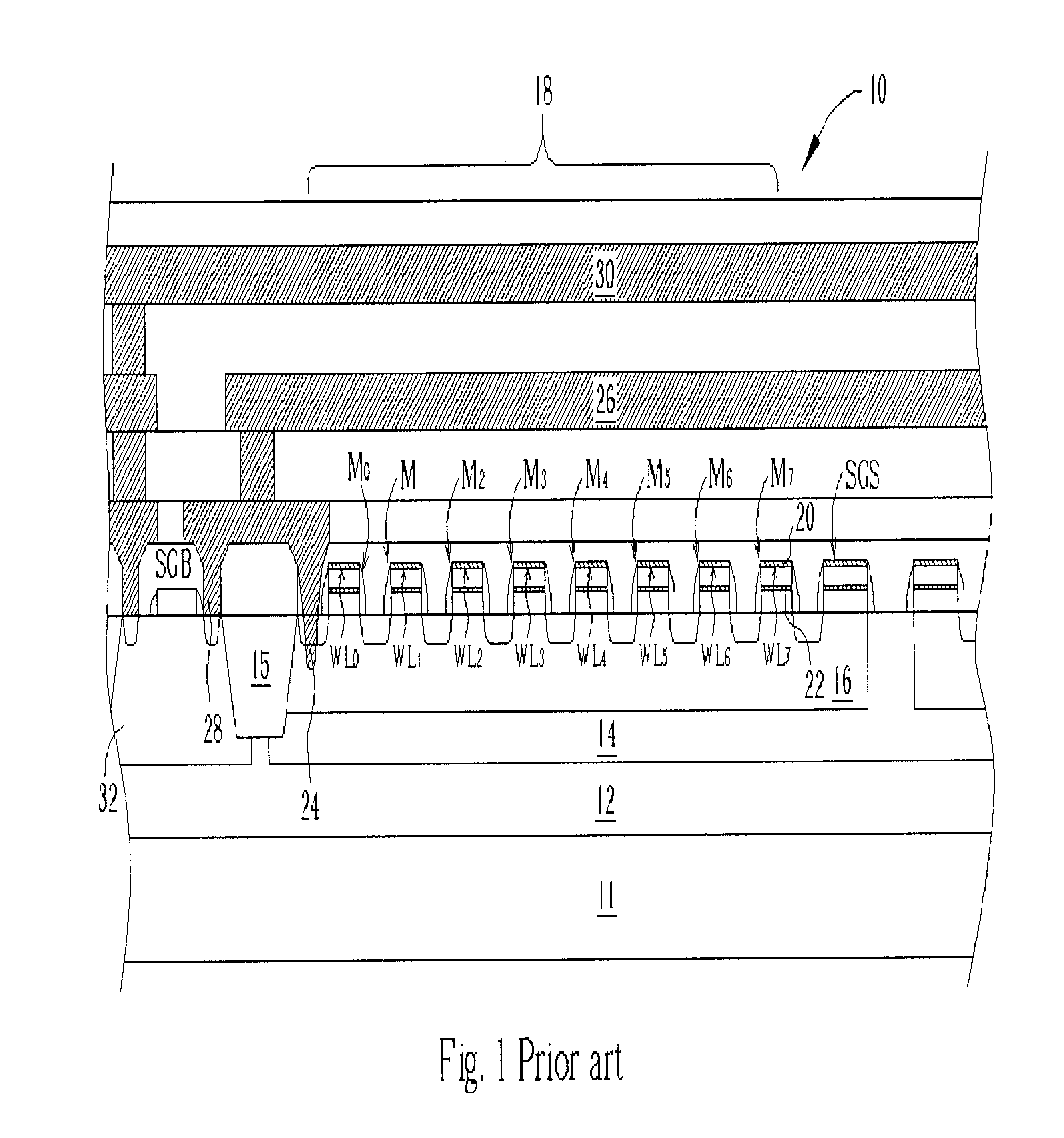
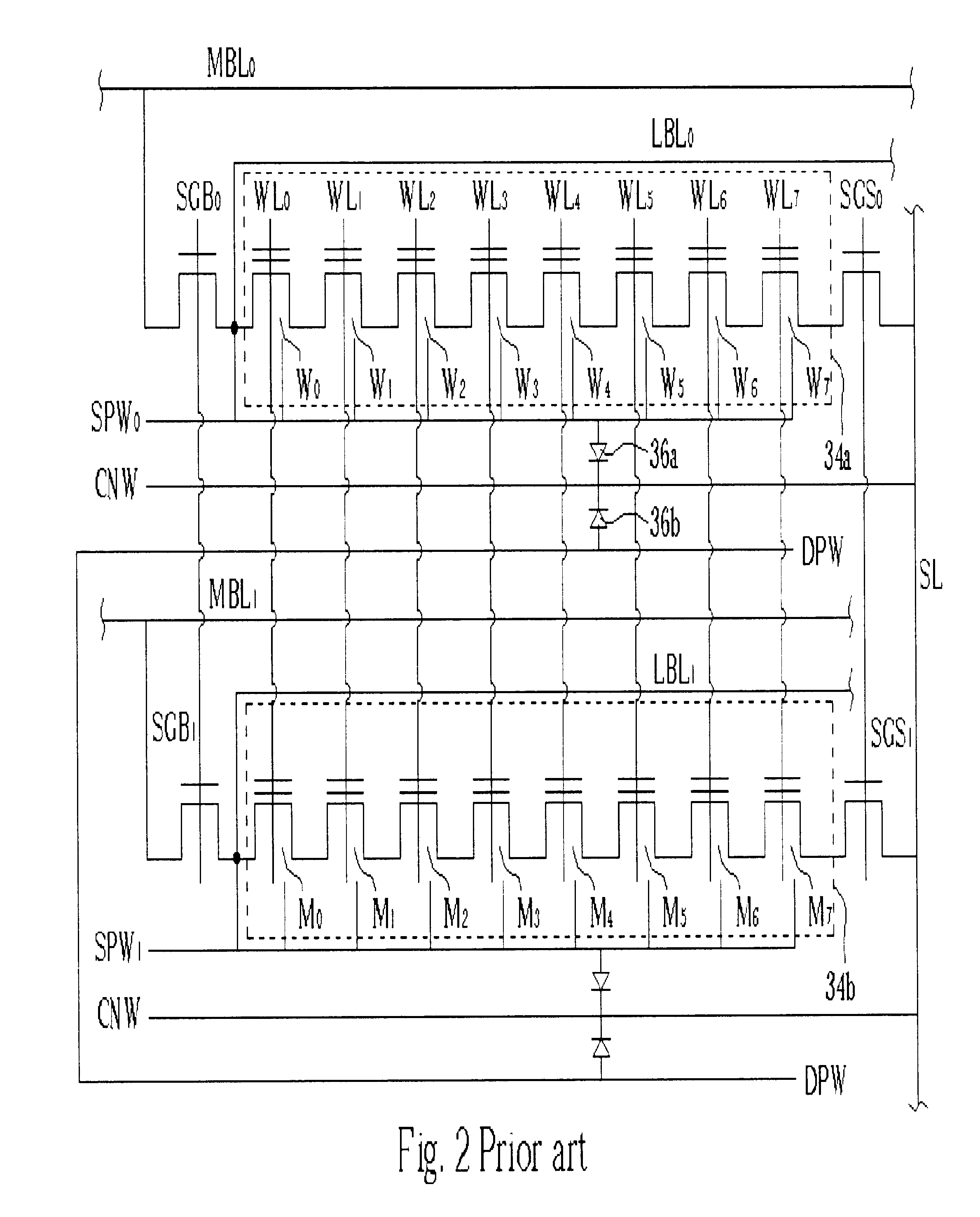
[0020]Please refer to FIG. 3 in conjunction with FIG. 2. FIG. 3 is a timing diagram illustrating operations of programming a flash memory according to the present invention. The method of programming a flash memory according to the present invention is applied to the flash memory 10 shown in FIG. 1 and FIG. 2. Because the component structure shown in FIG. 1 and the circuit structure shown in FIG. 2 are clearly described before, the lengthy description is not repeated. Suppose that the cell transistor M3 within the memory cell string 34b shown in FIG. 2 needs to be programmed for recording data. At T0, the voltage level of the source line SL is first raised from 0V toward a low voltage level Vcc. In the preferred embodiment, the low voltage level Vcc is a voltage level (3.3V for example) provided by an external power supply when the flash memory 10 works. At T1, the voltage levels of the control gates of the main bit line selecting transistors SGB0, SGB1 are raised from 0V toward the...


PUM


Abstract

A method of programming a flash memory through boosting a voltage level of a source line. The flash memory has n memory cell transistors cascaded in series, a local bit line positioned above the n memory cell transistors, a buried bit line positioned under the n memory cell transistors, and a source line positioned under the buried bit line. The method includes inputting a word line voltage to a control gate of a kth memory cell transistor, and after floating the local bit line, inputting a source line voltage to the source line for inducing an FN tunneling effect inside the kth memory cell transistor through capacitance coupling between the buried bit line and the source line.

Description

BACKGROUND OF INVENTION[0001]1. Field of the Invention[0002]The present invention relates to a method for programming a flash memory. In particular, the present invention discloses a method of programming a flash memory through boosting a voltage level of a source line.[0003]2. Description of the Prior Art[0004]Recently, the demand on portable electronic devices grows dramatically. Therefore, advanced technology associated with the flash memory or the electrically erasable programmable read-only memory (EEPROM) is developed, and the corresponding market is prosperous. The portable electronic devices include films of digital cameras and storage devices of cellular phones, video game apparatuses, and personal digital assistants, answering machines, and programmable ICs. The flash memory is a non-volatile memory, and it records data through altering a threshold voltage of a transistor (a memory cell) to control establishment of the conductive channel. In addition, the stored data are n...

Claims


Application Information

Patent Timeline
Patent Type & Authority Patents(United States)
IPC IPC(8): G11C11/34G11C16/04
CPCG11C16/10G11C5/145
Inventor YANG, CHING-SUNGCHANG, HSIANG-CHUNGWONG, WEI-ZHE
Owner POWERCHIP SEMICON CORP
Why Eureka
Try Eureka