LDMOS transistors and methods for making the same

a technology of mos transistors and fabrication methods, which is applied in the direction of semiconductor devices, basic electric elements, electrical equipment, etc., can solve the problems of limiting the drive current rating of the device, and the trade-off between rdson and bvdss, so as to reduce the on-state resistance and reduce the current flow. or inhibit the effect of restricting the current flow

Inactive Publication Date: 2005-05-31
TEXAS INSTR INC
View PDF12 Cites 114 Cited by
  • Summary
  • Abstract
  • Description
  • Claims
  • Application Information

AI Technical Summary

Benefits of technology

[0007]According to one aspect of the invention, methods are provided for fabricating LDMOS or other extended drain MOS transistors, wherein a source and a drain of a first conductivity type are formed in a substrate, such as a bulk semiconductor or SOI wafer. A gate structure is formed over a channel of a second opposite conductivity type, wherein the gate structure comprises a thick dielectric, a thin dielectric, and a conductive gate contact structure. The thick dielectric comprises a first end adjacent the drain and comprises a second opposite end that extends laterally toward the source. The thin dielectric extends over the substrate from the second end of the thick dielectric to the source, where the conductive gate contact structure extends over the thin dielectric and over a portion of the thick dielectric. The method further comprises increasing a concentration of dopants of the first conductivity type in an adjust region of the substrate proximate the second end of the thick dielectric at the transition between the thin and thick dielectrics. The inventor has found that this localized increase in dopants operates to reduce or inhibit current flow constriction as electrons move from the source to the drain at the transition from the thin dielectric to the thick dielectric, thereby reducing on-state resistance (e g., Rdson) without significant adverse impact to the breakdown voltage performance (e.g., BVdss) of the resulting transistor.

Problems solved by technology

In conventional drain-extended LDMOS devices, the Rdson and breakdown voltage are thus generally inversely related, wherein the drain extension causes an increase in Rdson, thus limiting the drive current rating of the device.
For LDMOS transistors, the tradeoffs between Rdson and BVdss present challenges to scaling efforts, particularly where the design specifications for breakdown voltage and current carrying capability remain the same or increase.

Method used


Image

  • LDMOS transistors and methods for making the same
  • LDMOS transistors and methods for making the same
  • LDMOS transistors and methods for making the same

Examples


Embodiment Construction

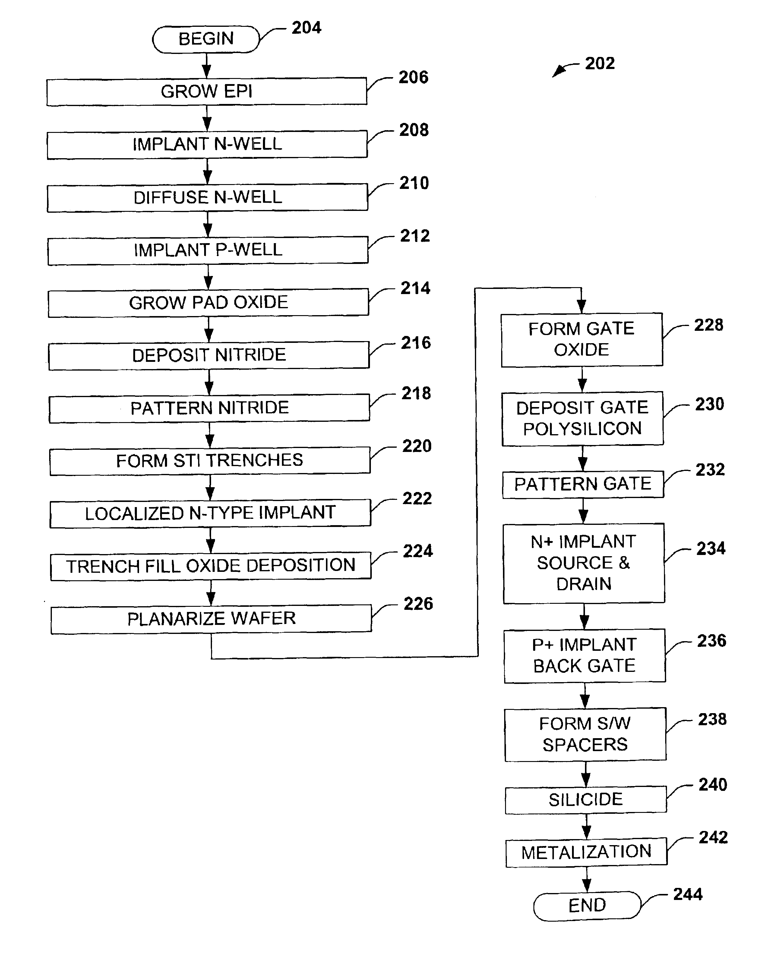
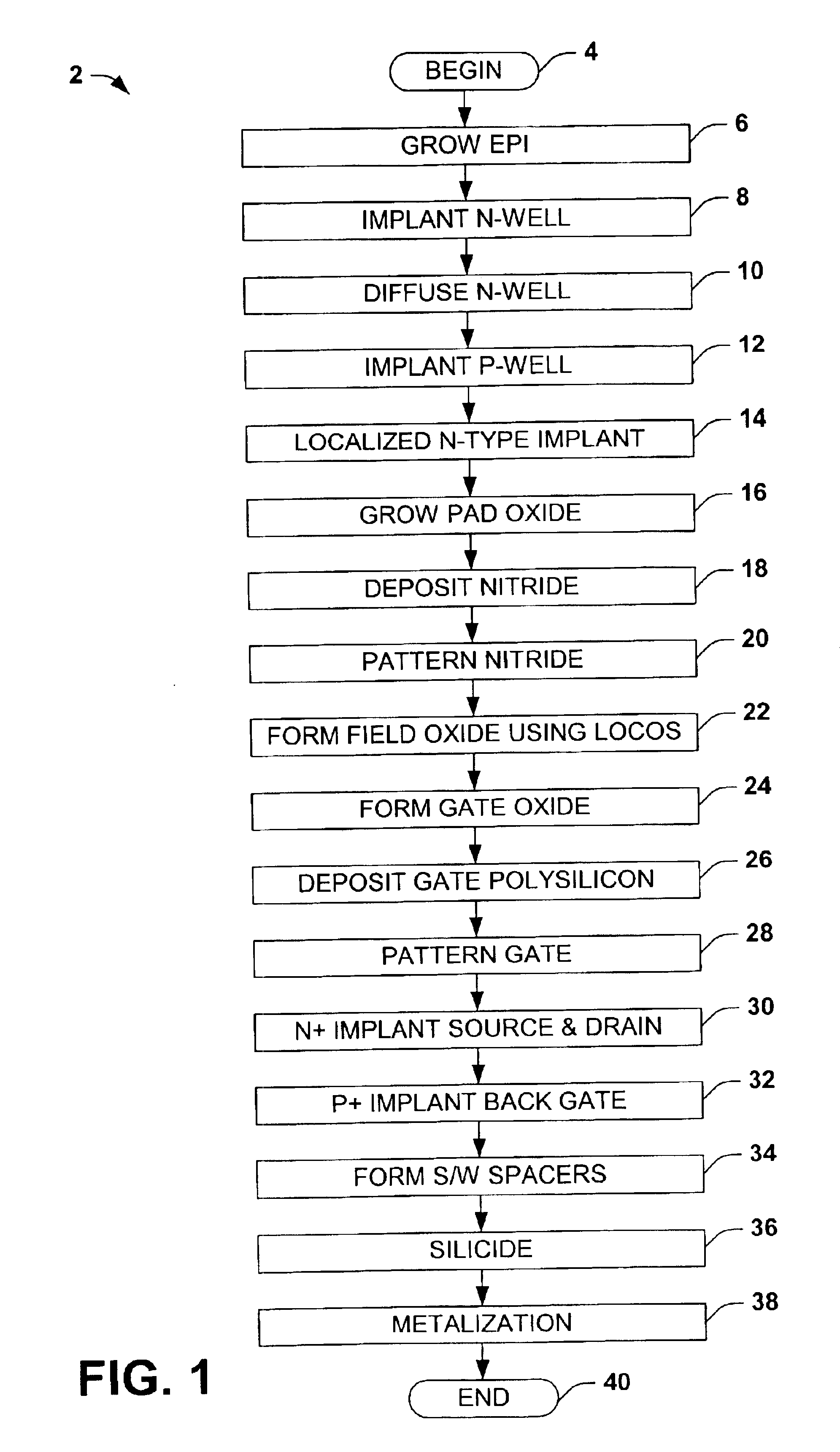
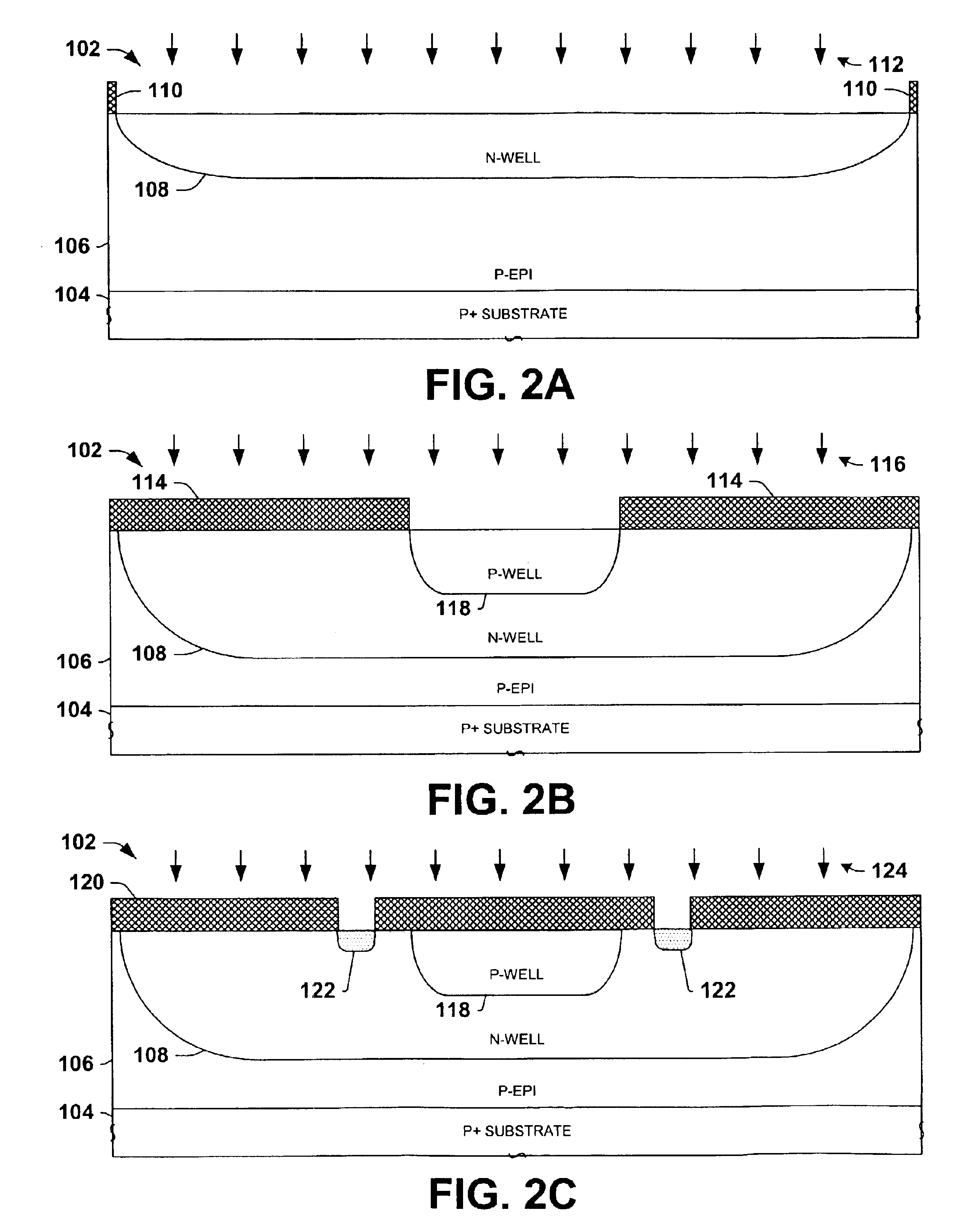
[0016]One or more implementations of the present invention will now be described with reference to the attached drawings, wherein like reference numerals are used to refer to like elements throughout. The invention provides for addition of extra dopants to a localized region of an LDMOS or other drain-extended MOS transistor to reduce on-state resistance (Rdson) without adversely impacting device breakdown voltage, which may be implemented in association with PMOS or NMOS type extended drain transistors. In the examples below, the various aspects of the invention are illustrated and described with respect to exemplary n-channel LDMOS type transistors fabricated using p-type silicon substrates with a p-type epitaxial layer formed thereover. However, the invention is not limited to the illustrated examples, wherein NMOS or PMOS transistors may be fabricated using any type of substrate, including but not limited to silicon or SOI wafers, and wherein all such variants are contemplated a...


PUM


Abstract

LDMOS transistor devices and fabrication methods are provided, in which additional dopants are provided to region of a substrate near a thick dielectric between the channel and the drain to reduce device resistance without significantly impacting breakdown voltage. The extra dopants are added by implantation prior to formation of the thick dielectric, such as before oxidizing silicon in a LOCOS process or following trench formation and before filling the trench in an STI process.

Description

FIELD OF INVENTION[0001]The present invention relates generally to semiconductor devices and more particularly to extended-drain MOS transistor devices and fabrication methods for making the same.BACKGROUND OF THE INVENTION[0002]Power semiconductor products are often fabricated using extended-drain N or P channel transistors, such as lateral double-diffused metal-oxide-semiconductor (LDMOS) devices for high power switching applications. LDMOS devices advantageously combine short-channel operation with high current handling capabilities and are able to withstand large blocking voltages without suffering voltage breakdown failure. Accordingly, these devices are ideally suited for power switching applications, particularly where inductive loads are to be driven. N channel LDMOS transistors are asymmetrical devices in which a p-type channel region is typically formed in a p-well between an n-type source and an extended n-type drain. Low n-type doping on the drain side provides a large d...

Claims


Application Information

Patent Timeline
Patent Type & Authority Patents(United States)
IPC IPC(8): H01L21/02H01L21/336H01L29/78H01L29/66H01L21/265H01L29/08H01L29/423H01L29/02H01L29/40
CPCH01L29/7816H01L29/66689H01L21/26586H01L29/0878H01L29/42368H01L29/4933H01L29/665H01L29/456
Inventor LIN, JOHN
Owner TEXAS INSTR INC
Why Eureka
Try Eureka