

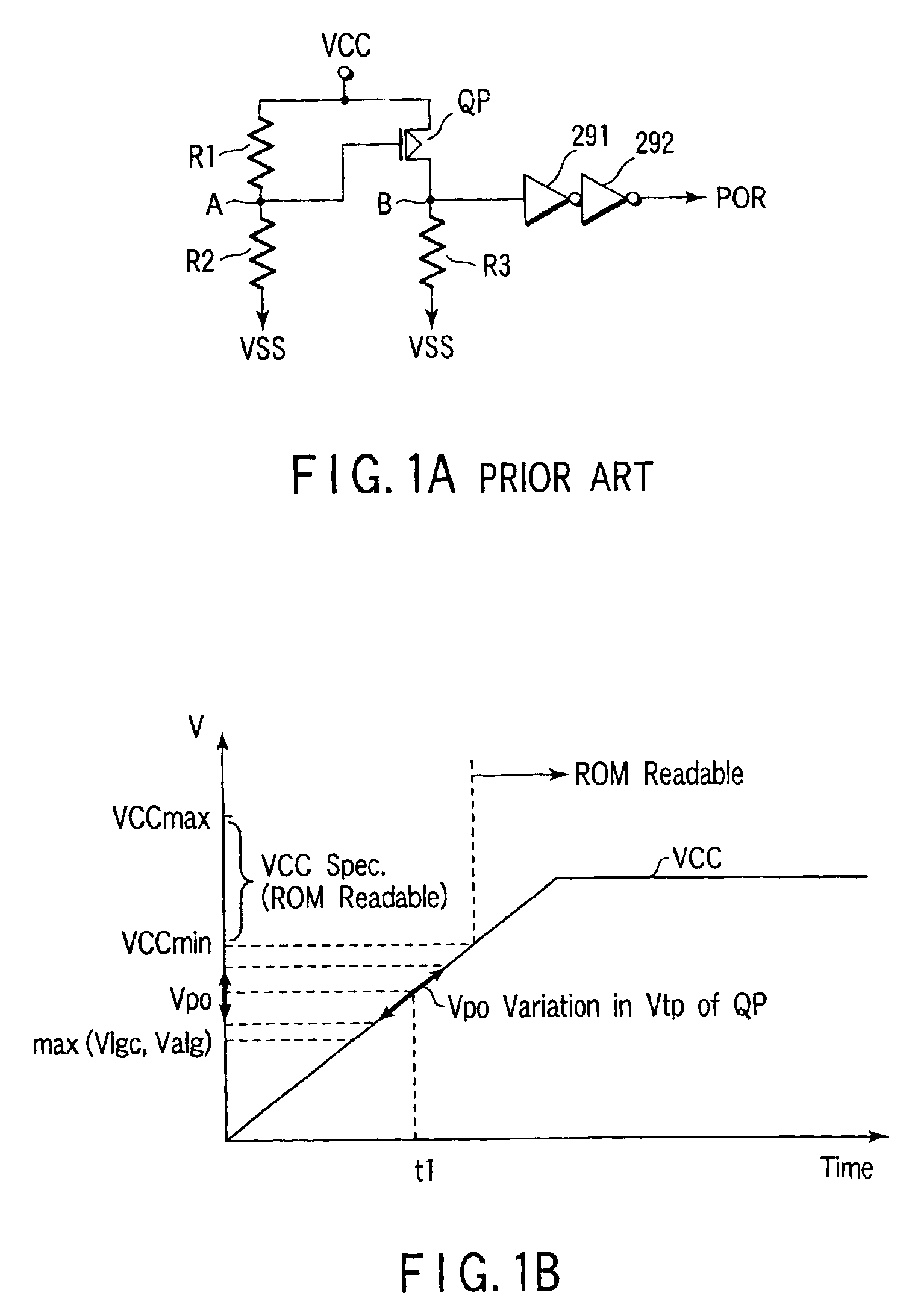
Semiconductor memory device having a power-on reset circuit
a technology of reset circuit and memory device, which is applied in the direction of electronic switching, pulse technique, instruments, etc., can solve the problem of basically impossible use of such a low power supply voltag
- Summary
- Abstract
- Description
- Claims
- Application Information
AI Technical Summary
Benefits of technology
Problems solved by technology
Method used
Image

Examples
first embodiment
(First Embodiment)
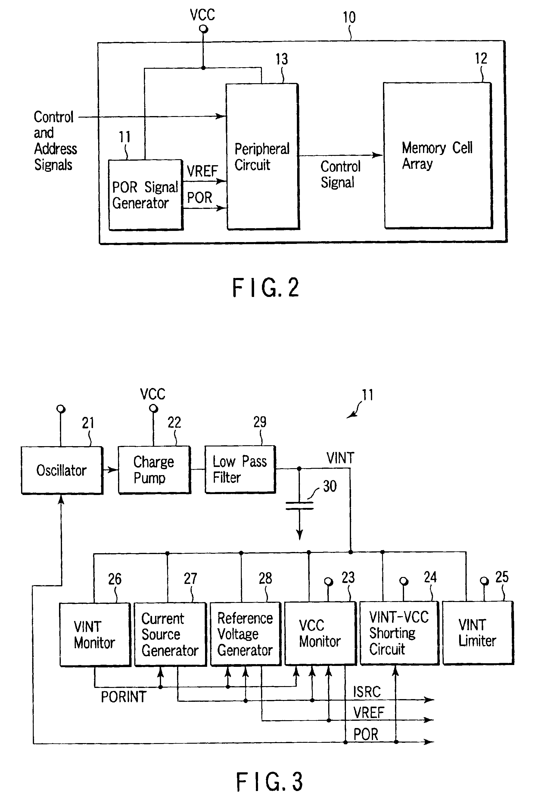
[0072]FIG. 2 schematically shows the arrangement of a semiconductor memory according to the first embodiment of the present invention.
[0073]Referring to FIG. 2, a power supply voltage VCC and control and address signals are externally input to a memory chip 10. In the chip, a POR signal generator (power-on reset circuit) 11, memory cell array 12, and peripheral circuit 13 for controlling the memory cell array 12 are arranged. The POR signal generator 11 receives the power supply voltage VCC and generates a reference voltage VREF and power-on reset signal POR. The peripheral circuit 13 receives the control and address signals and also the reference voltage VREF and power-on reset signal POR.
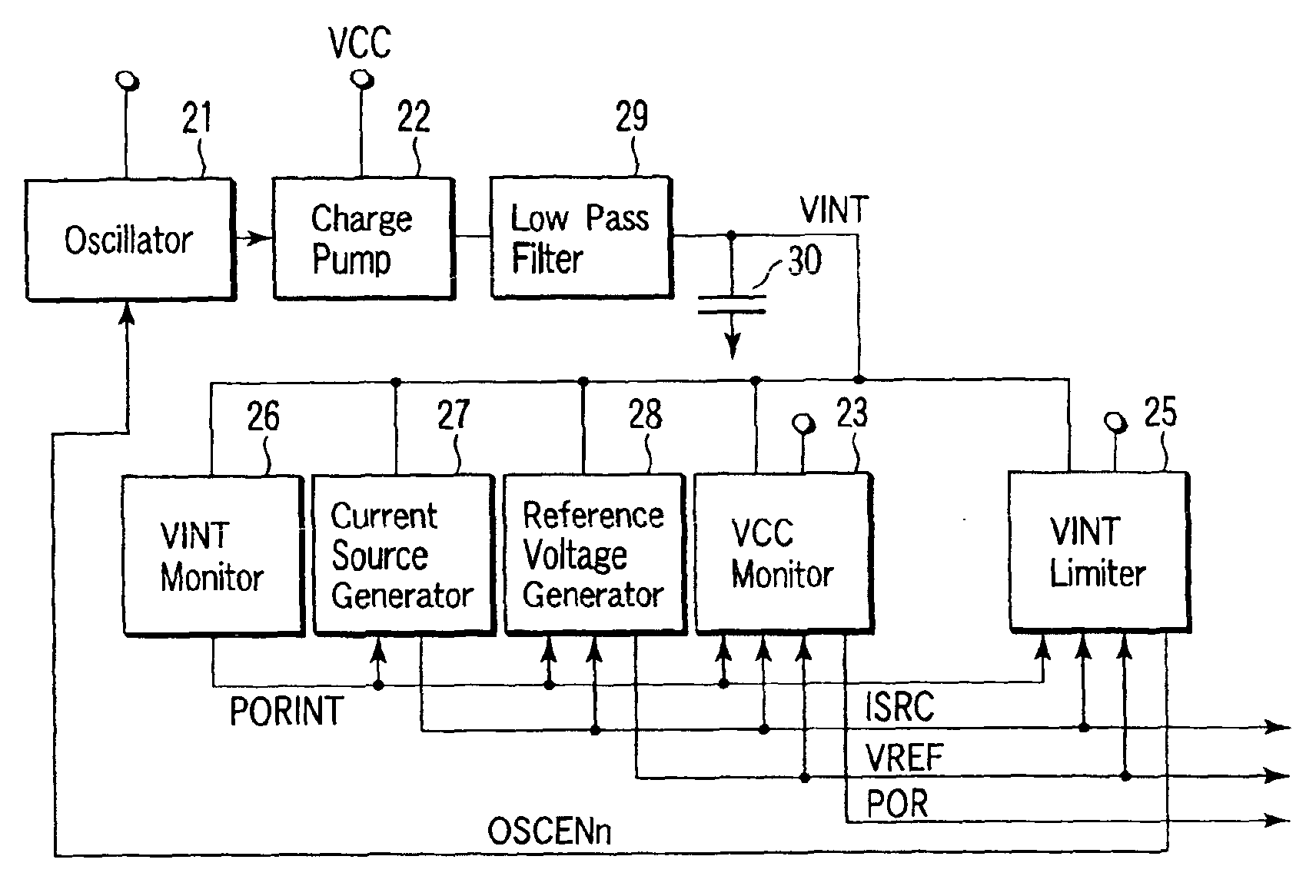
[0074]FIG. 3 is a block diagram showing the first example of the POR signal generator 11 in FIG. 2.
[0075]This POR signal generator includes circuits using the power supply voltage VCC as a power supply and circuits using a charge-pumped voltage VINT charge-pumped from the power s...
second embodiment
(Second Embodiment)
[0141]The power-on reset signal generation scheme of the present invention can also be applied to a voltage down converter system in a semiconductor device. A semiconductor memory according to the second embodiment, which uses a voltage down converter system, will be described below.
[0142]FIG. 17 schematically shows the arrangement of a memory chip 10a of the semiconductor memory according to the second embodiment of the semiconductor device of the present invention.
[0143]The memory chip 10a is the same as the memory chip 10 described above with reference to FIG. 2 except that a voltage down converter 14 which generates a dropped power supply voltage VDD from a power supply voltage VCC and reference voltage VREF and supplies the dropped power supply voltage VDD to a peripheral circuit 13 as a main power supply is added, and the same reference numerals as in FIG. 2 denote the same parts in FIG. 17.
[0144]In a memory using such a voltage down converter system, a powe...
third embodiment
(Third Embodiment)
[0201]FIG. 32 is a block diagram showing the basic arrangement of a nonvolatile semiconductor memory device according to the third embodiment.
[0202]As shown in FIG. 32, nonvolatile memory cells (not shown) are arrayed in a matrix in a memory cell array 301. A part of the memory cell array 301 is used as a ROM fuse area 302. Memory cells in the ROM fuse area 302 store fuse data such as the address data of defective cells in the memory cell array 301 and voltage setting data for correcting a variation unique to the chip. Each memory cell is formed from, e.g., a MOSFET with a variable threshold value, which has a floating gate and stores data in accordance with a threshold value.
[0203]An address buffer 303 outputs a row address RADD and column address CADD. The row address RADD is supplied to a row decoder 304, and the column address CADD is supplied to a column decoder 305.
[0204]The row decoder 304 selects a row of the memory cell array 301 on the basis of the receiv...
PUM
 Abstract
Description
Claims
Application Information