Qualifying patterns, patterning processes, or patterning apparatus in the fabrication of microlithographic patterns

Inactive Publication Date: 2005-06-07
KLA TENCOR CORP
View PDF7 Cites 150 Cited by
  • Summary
  • Abstract
  • Description
  • Claims
  • Application Information

AI Technical Summary

Benefits of technology

[0008]A preferred implementation of the present invention is a method of qualifying incoming reticles and process conditions on test wafers to maximize the available usable process window for a given reticle exposure tool combination. The method qualifies the image produced by the cumulative effect of various configurations of illumination sources, optical proximity correction artifacts, phase shifted imaging, and various photochemical processing techniques implemented at the imaging plane. Practicing this method on test wafers enables the identification of spatial areas where a process will fail first and candidate regions for carrying out defect inspection and metrology.
[0009]The nature of process window qualification is to induce pattern anomalies, such as transient repeating defects, by varying a process parameter or operating variable. O

Problems solved by technology

Although they are implemented in semiconductor device designs to facilitate low k1 lithography, these RET make reticles more difficult and consequently more expensive to manufacture.
Marginal RET designs not noted by simulation checks translate into electrical failures in wafer fabrication, affect yield, and possibly remain unnoticed until wafer fabrication is complet

Method used


Image

  • Qualifying patterns, patterning processes, or patterning apparatus in the fabrication of microlithographic patterns
  • Qualifying patterns, patterning processes, or patterning apparatus in the fabrication of microlithographic patterns
  • Qualifying patterns, patterning processes, or patterning apparatus in the fabrication of microlithographic patterns

Examples


Embodiment Construction

[0025]A preferred embodiment of the invention implements modulation of focus of light illuminating reticles, each of which is used to expose by a step and repeat or a step and scan process a top layer of photoresist covering a test wafer. The reticles are printed on optimized film stacks, the type of optimization depending on the type of process level, which includes contact or vias, gate, and trench. The base film stack is preferably a simple thermally grown or deposited stack of 1050 Å oxide covered by 320 Å SiON.

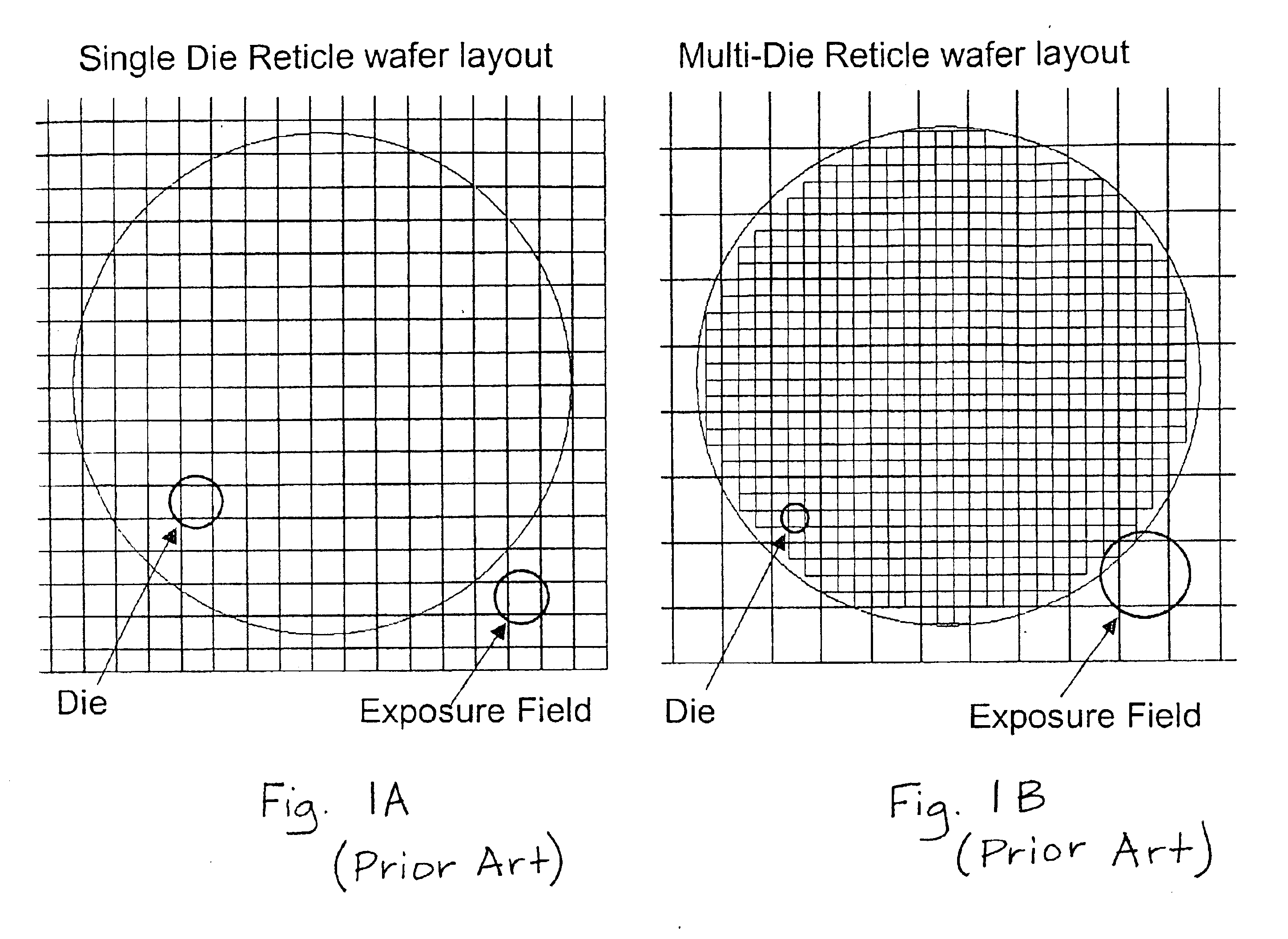
[0026]FIGS. 1A and 1B show, respectively, prior art single die reticle (exposure field contains one unique die) and prior art multi-die reticle (array of multiple rows and columns of nominally identical die) wafer layouts and indicate their exposure field and die boundary dimensions. After photoresist patterning, inspection is preferably, but need not be, performed after etching on the SiON / oxide base film stack and stripping the photoresist. Inspecting an etched pattern ...


PUM


Abstract

The invention is a method of determining the presence of an anomaly in qualifying a pattern, patterning process, or patterning apparatus used in the fabrication of microlithographic patterns. A preferred implementation of the method qualifies incoming reticles and process conditions on test wafers to maximize the available usable process window for a given reticle exposure tool combination. Practicing this method on test wafers enables the identification of spatial areas where a process will fail first and candidate regions for carrying out defect inspection and metrology. Other preferred implementations of the method qualify masks, reticles, or other patterns characterized by data bases on which are stored image data acquired by practice of aerial image measurement system (AIMS) or design rule checking (DRC) techniques.

Description

RELATED APPLICATION[0001]This application claims benefit of U.S. Provisional Patent Application No. 60 / 396,197, filed Jul. 15, 2002.TECHNICAL FIELD[0002]This invention relates to the manufacture of microelectronic devices and, in particular, to a method of qualifying a pattern, patterning process, or patterning apparatus used in the fabrication of microlithographic patterns for producing microelectronic devices.BACKGROUND OF THE INVENTION[0003]The rapid decrease in k1 (line-width=k1 (λ / NA)) in lithographic manufacture of semiconductor devices has necessitated the use of Resolution Enhancement Techniques (RET). These RET include, but are not limited to, Optical Proximity Corrections (OPC), Phase Shift Masks (PSM), and assist bar corrections. Although they are implemented in semiconductor device designs to facilitate low k1 lithography, these RET make reticles more difficult and consequently more expensive to manufacture.[0004]Semiconductor device design and reticle manufacturing qual...

Claims


Application Information

Patent Timeline
IPC IPC(8): G03F9/00G03F9/02G03F7/207G03F7/22G03F7/23
CPCG03F1/84G03F7/7065G03F7/70641
Inventor PETERSON, INGRID B.HOFF, MIKE VON DEN
Owner KLA TENCOR CORP
Why Eureka
Try Eureka