Probing of device elements

Inactive Publication Date: 2005-06-07
TAIWAN SEMICON MFG CO LTD
View PDF6 Cites 116 Cited by
  • Summary
  • Abstract
  • Description
  • Claims
  • Application Information

AI Technical Summary

Benefits of technology

[0014]In accordance with these and other objects and advantages, the present invention is generally directed to a new and improved method for the probing of integrated circuits (ICs) and is particularly suitable for probing various elements of an IC for failure analysis or other electrical testing and/or measurement of the IC. The method includes providing a probe access trench in the IMD (intermetal dielectric) or other s

Problems solved by technology

However, one of the limitations of using the probing pad is that the probing pad introduces a relatively high contact resistance into the electrical conduction between the metal line or other element and the test probe.
This may result in attenuated electrical signals that are picked up by the test probe and translate into faulty test data obtained from the device.
This causes electrical bridging and leakag

Method used


Image

  • Probing of device elements
  • Probing of device elements
  • Probing of device elements

Examples


Embodiment Construction

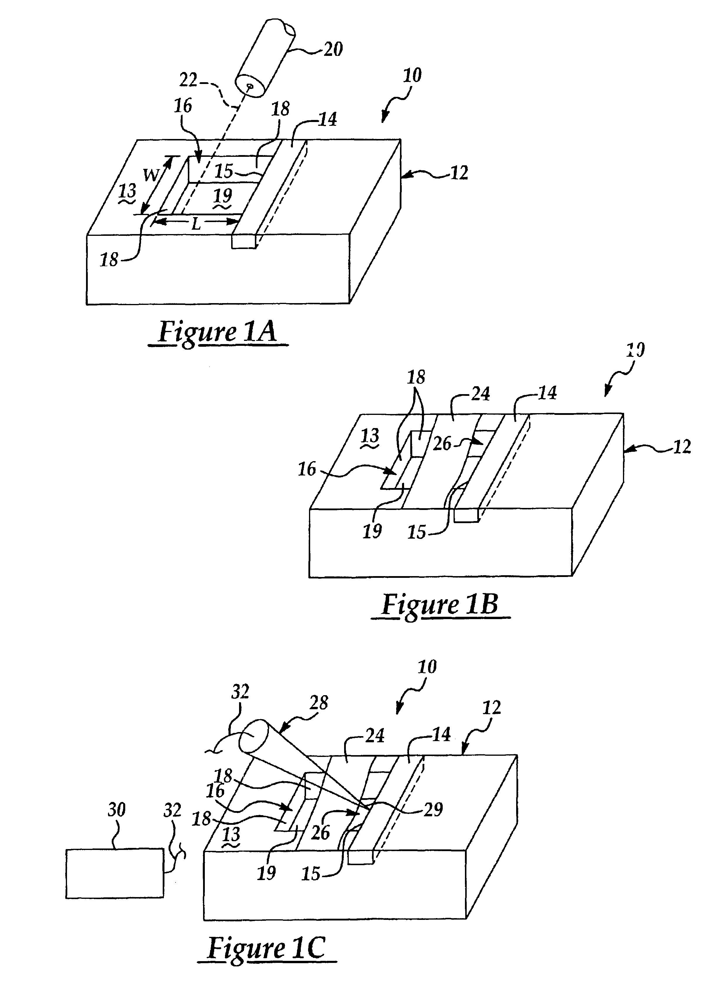
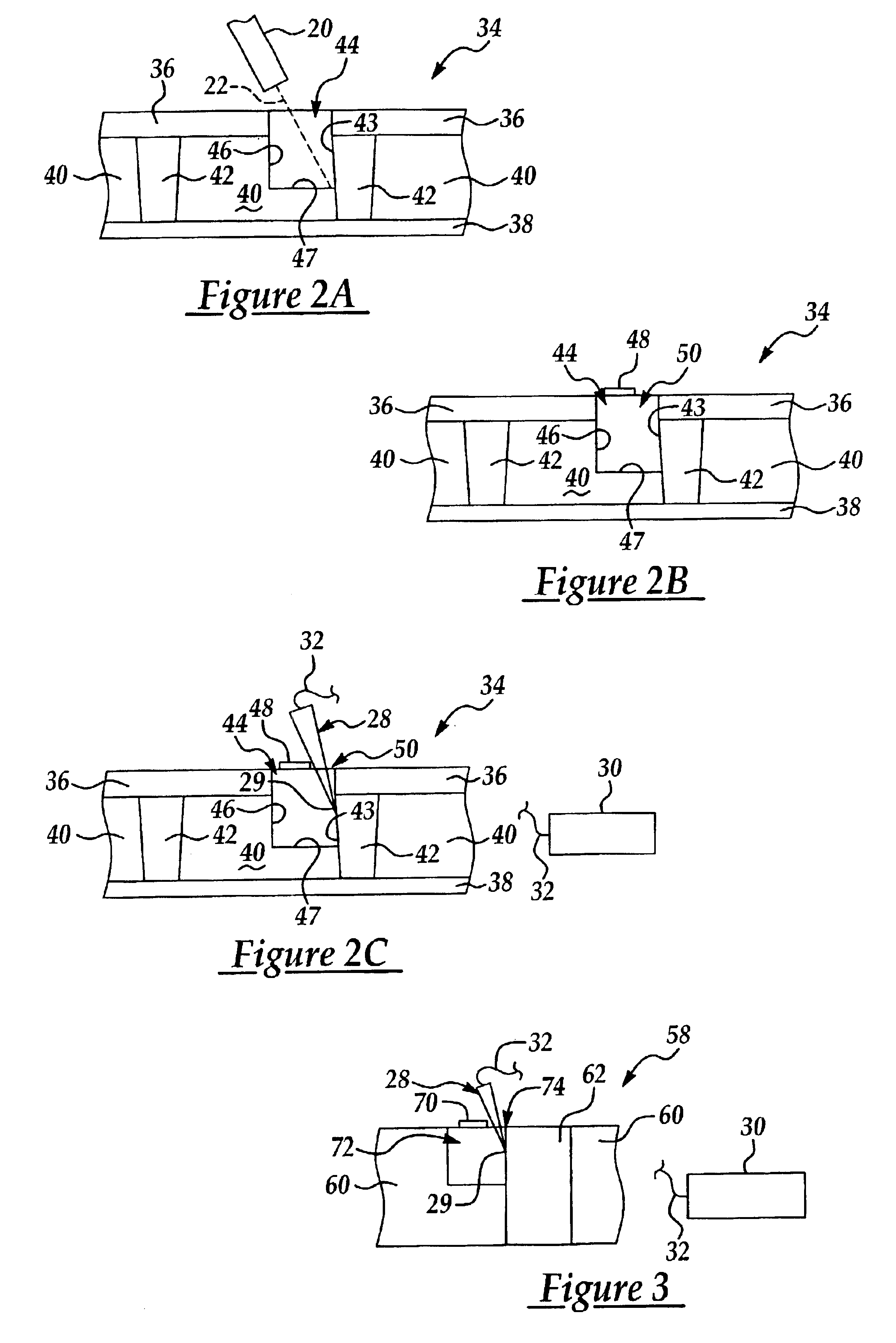
[0025]The methods of the present invention are suitable for probing an IC device preparatory to carrying out a variety of electrical tests and / or measurements, including failure analysis, for example, on the device without the need for interposing a probing pad between a test probe and the various elements of the integrated circuit to be contacted with the probe. The IC elements which may be contacted by the probe for the various electrical tests may include metal lines, contact vias or p / n junctions, in non-exclusive particular. Direct electrical contact between the test probe and the element avoids the excessively high contact resistance which is characteristic of the conventional test probing method in which the probing pad is interposed between the probe tip and the element during testing.

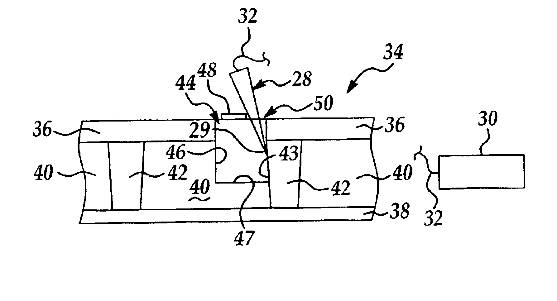
[0026]Referring initially to FIGS. 1A-1C, a section of an IC device 10 taken from a wafer (not shown) includes a metal line 14 that connects circuit elements such as transistors, resistors and ...


PUM


Abstract

A new and improved method for the probing of integrated circuits (ICs) and is particularly suitable for probing various elements of an IC for failure analysis or other electrical testing and/or measurement of the IC. The method includes providing a probe access trench in the IMD (intermetal dielectric) or other substrate adjacent to the circuit element to be tested and then providing direct electrical contact between the test probe and the sidewall of the element through the trench, during the testing process. Such direct electrical contact between the test probe and the sidewall of the element prevents excessively high contact resistance which may otherwise occur in the use of a probing pad between the test probe and the element.

Description

FIELD OF THE INVENTION[0001]The present invention relates to IC metrology and defect inspection techniques used in the inspection of defects in WIP (work-in-progress) wafers during the fabrication of semiconductor integrated circuits. More particularly, the present invention relates to probing of elements such as metal lines or vias in a microelectronic device by forming a probe access trench adjacent to the element and accessing the element with a test probe through the trench to prevent the need for forming a probing pad on the element and contacting the element through the probing pad.BACKGROUND OF THE INVENTION[0002]The fabrication of various solid state devices requires the use of planar substrates, or semiconductor wafers, on which integrated circuits are fabricated. The final number, or yield, of functional integrated circuits on a wafer at the end of the IC fabrication process is of utmost importance to semiconductor manufacturers, and increasing the yield of circuits on the...

Claims


Application Information

Patent Timeline
IPC IPC(8): G01R31/28
CPCG01R31/2884
Inventor SUN, LUEN-CHIAN
Owner TAIWAN SEMICON MFG CO LTD
Why Eureka
Try Eureka