Light-emitting diode with cavity containing a filler

a filler and diode technology, applied in the direction of basic electric elements, electrical equipment, semiconductor devices, etc., can solve the problems of affecting the brightness of leds, so as to reduce manufacturing costs and improve light intensity.

Inactive Publication Date: 2005-06-07
OPTO TECH
View PDF8 Cites 30 Cited by
  • Summary
  • Abstract
  • Description
  • Claims
  • Application Information

AI Technical Summary

Benefits of technology

[0013]Accordingly, it is the primary object of the present invention to provide a light-emitting diode and a method for manufacturing such a light-emitting diode, so as to improve the light intensity and reduce the manufacturing cost.
[0014]It is another object of the present invention to provide a light-emitting diode and a method for manufacturing such a light-emitting diode, in which an opposed electrode surrounding the bottom edge of the epitaxial LED layer is used to conduct the electric current towards the entire epitaxial LED layer such that the P-N junction is uniformly employed as a light source and the optical path for the light source is shortened, enhancing the LED brightness.
[0015]It is still another object of the present invention to provide a light-emitting diode and a method for manufacturing such a light-emitting diode, in which a transparent material is used as the substrate such that the light emitted from the P-N junction travels through the substrate, increasing the flexibility of the chosen materials and thus reducing the cost.

Problems solved by technology

When a direct band-gap III-V compound semiconductor material such as GaAs is used as a substrate of an LED, the GaAs substrate absorbs a considerable amount of incident light and adversely affects the brightness of the LED.
However, using such an indirect band-gap material complicates the manufacturing process because it suffers from poor light-emitting efficiency and needs to be doped with some impurities to improve the efficiency through lattice vibration or dispersion centers.
As a result, the manufacturing cost is increased when the indirect band-gap material is used for the LED.
Moreover, the P-N junction of the LED is not uniformly used.3. The conductive substrate limits the chosen materials, which may be unfavorable for cost down.

Method used


Image

  • Light-emitting diode with cavity containing a filler
  • Light-emitting diode with cavity containing a filler
  • Light-emitting diode with cavity containing a filler

Examples


Embodiment Construction

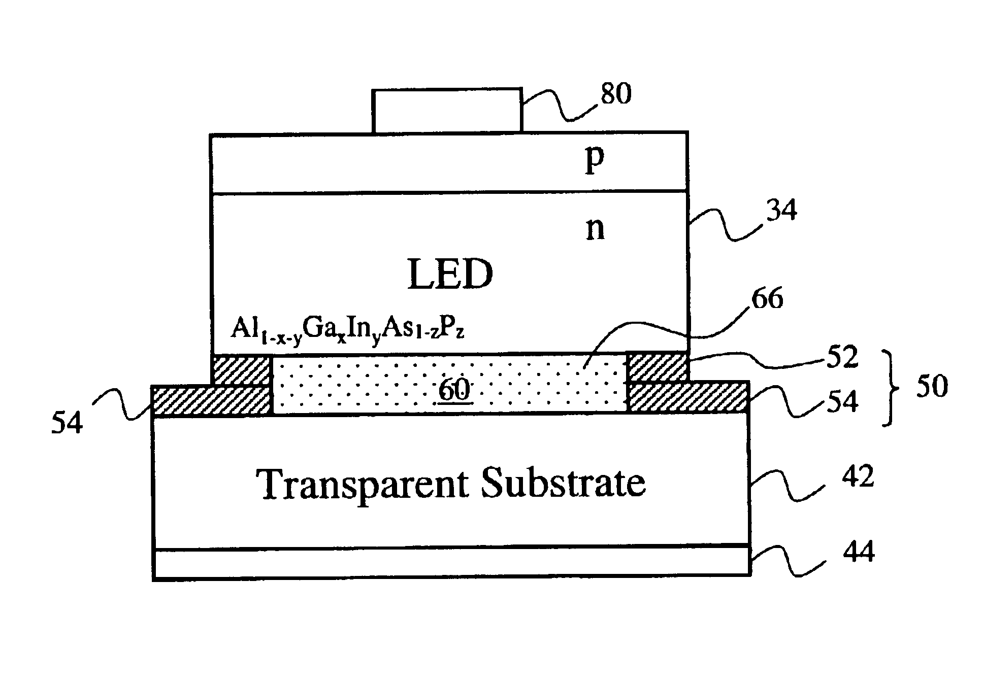
[0026]The present invention providing a light-emitting diode with enhanced brightness and a method for manufacturing the same can be exemplified by the preferred embodiments as described hereinafter.

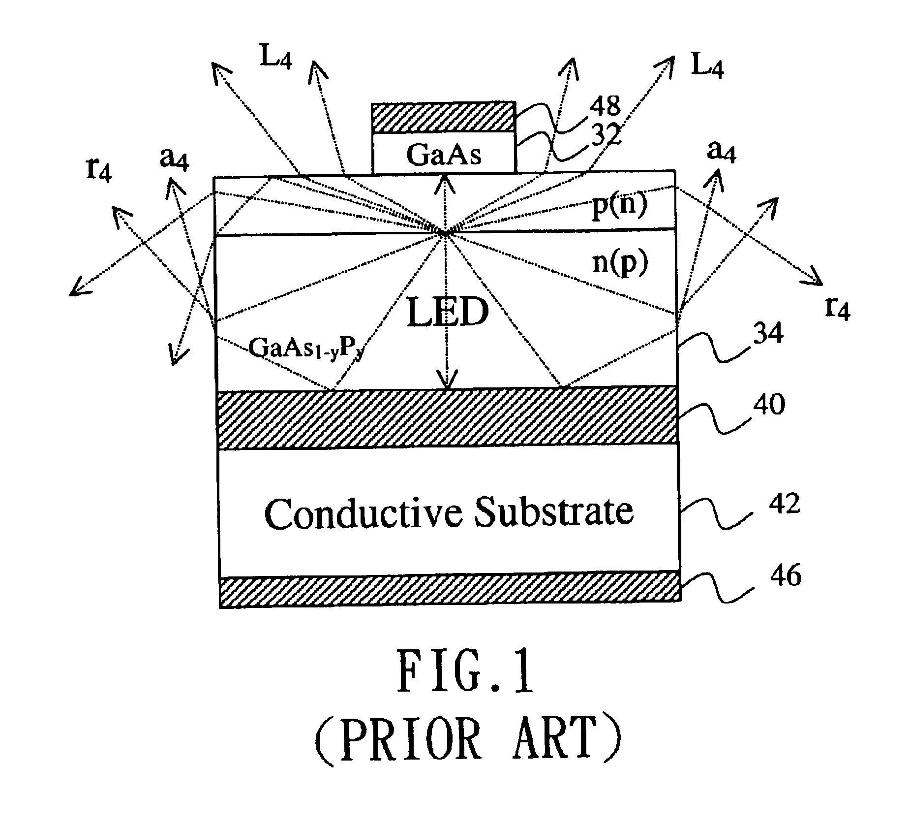
[0027]To start with, please refer to FIG. 2A to FIG. 2F, which are cross-sectional views showing the manufacturing process for an LED in accordance with one embodiment of the present invention. The LED with a direct band-gap III-V compound semiconductor material such as AlGaInAsP is formed on a GaAs substrate. Therefore, the method according to the present invention includes the following steps.

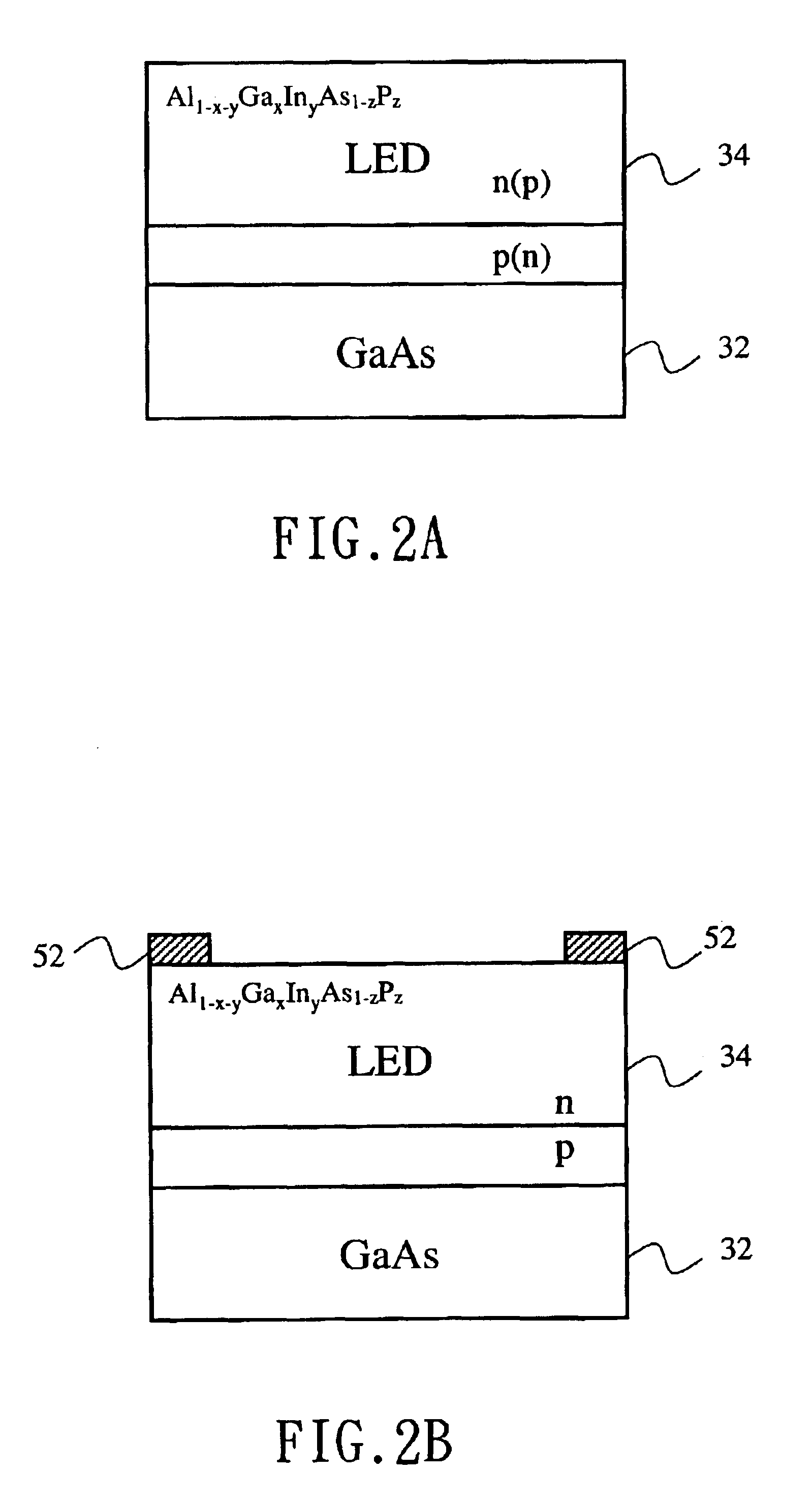
[0028]Step 1: An epitaxial LED layer 34 having a P-N junction (or n-p junction as shown in the brackets in FIG. 2A) is formed on a GaAs substrate 32, as shown in FIG. 2A.

[0029]Step 2: A first conductive electrode 52 is formed by depositing technology on the epitaxial LED layer 34 where the epitaxial LED layer 34 is not connected to the GaAs substrate 32, as shown in FIG. 2B.

[0030]Step 3: A second ...


PUM

PropertyMeasurementUnit
conductiveaaaaaaaaaa
transparentaaaaaaaaaa
heightaaaaaaaaaa

Abstract

The present invention discloses a light-emitting diode and a method for manufacturing such a light-emitting diode with a direct band-gap III-V compound semiconductor material on a GaAs substrate. It is implemented by forming a first conductive electrode on the top edge of the epitaxial LED layer and a second conductive electrode opposite the first conductive electrode on the edge of a transparent substrate. Further, after the first conductive electrode and second conductive electrode are connected by chip bonding skill, it is selectively to remove the GaAs substrate and plate a transparent electrode on the top portion of the epitaxial LED layer. Therefore, when casting from P-N junction of the light-emitting diode, the light will go through with directions of the top portion of epitaxial layer and transparent substrate.

Description

BACKGROUND OF THE INVENTION[0001]1. Field of the Invention[0002]The present invention generally relates to a light-emitting diode and a method for manufacturing the same and, more particularly, to a light-emitting diode with enhanced brightness and a method for manufacturing such a light-emitting diode with a direct band-gap III-V compound semiconductor material on a GaAs substrate. The present invention relates to an improvement to Taiwan Patent Publication No. 41516 “Light-emitting diode with enhanced brightness and method for fabricating the same” filed by the inventors of present invention.[0003]2. Description of the Prior Art[0004]The light-emitting diode (to be abbreviated as LED hereinafter) has received considerable attention for its advantages such as long lifetime, small size, low heat generation, low power consumption, high response speed, monochromic lighting ability, etc. and has been widely used in applications such as computer peripherals, clock displays, display pane...

Claims


Application Information

Patent Timeline
Patent Type & Authority Patents(United States)
IPC IPC(8): H01L33/00H01L33/38
CPCH01L33/0079H01L33/38H01L24/32H01L33/505H01L33/62H01L33/387H01L2924/12041H01L33/0093H01L2924/00
Inventor LIN, MING-DERTSAI, CHANG-DA
Owner OPTO TECH
Why Eureka
Try Eureka