Method for improving chip yields in the presence of via flaring

a technology of via flaring and chip yield, which is applied in the field of reducing via shorts on integrated circuits, can solve the problems of reducing the yield of conventional integrated circuit manufacturing technologies, removing all via shapes in the design, and reducing the time-consuming and costly redesign of integrated circuits

Inactive Publication Date: 2005-06-07
IBM CORP
View PDF7 Cites 8 Cited by
  • Summary
  • Abstract
  • Description
  • Claims
  • Application Information

AI Technical Summary

Benefits of technology

[0008]In order to attain the objects suggested above, there is provided, according to one aspect of the invention, a modification procedure that reduces errors on an integrated circuit due to via shorts while at the same time avoiding the un-nesting of the layout design and thereby permitting verification of the layout design by standard LVS verification tools.

Problems solved by technology

Conventional integrated circuit manufacturing technologies suffer from reduced yields due to via shorts, i.e., electrical shorts.
A redesign of an integrated circuit is time consuming and costly.
However, for example, in a hierarchical shapes database where one cell contains all the via shapes of the database, a conventional shape algorithm may result in the deletion of all via shapes in the design.
However, the flat design layout is impossible to compare to the design schematic, i.e., using standard layout versus schematic (hereinafter LVS ) verification methods, since the design schematic hierarchy is different from the design layout hierarchy.

Method used


Image

  • Method for improving chip yields in the presence of via flaring
  • Method for improving chip yields in the presence of via flaring
  • Method for improving chip yields in the presence of via flaring

Examples


Embodiment Construction

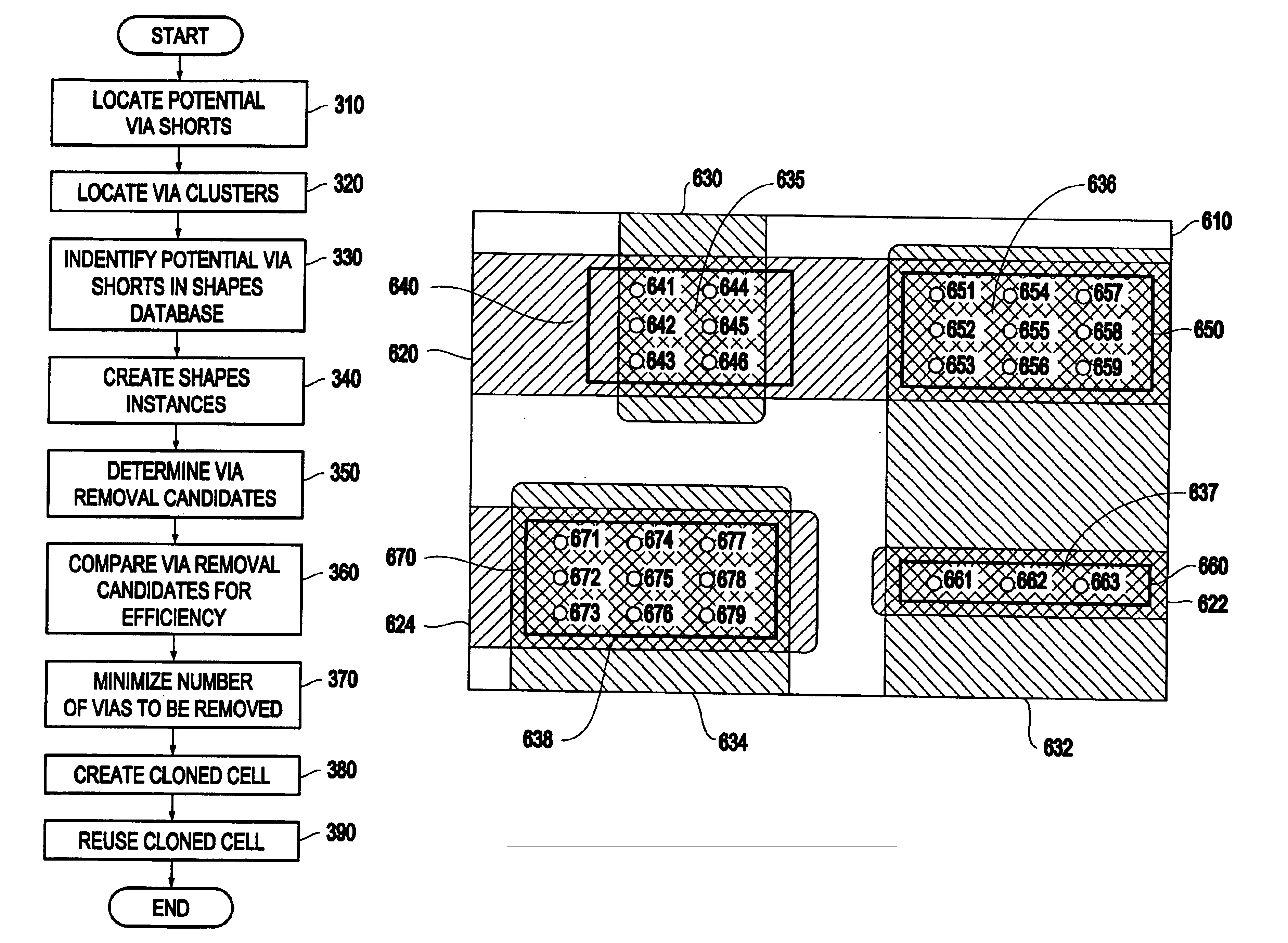
[0024]The design and manufacture of integrated circuits utilize shape databases. A shape database is made up of various database elements (or database objects), such as, but not limited to, manufacturing layers or levels (such as, but not limited to, polysilicon, metal1, via1, etc.) and geometric shapes (such as, but not limited to, rectangles, polygons, etc.). Each shape can be assigned to a specific layer, named cells (which contain shapes in a local coordinate system), and / or cell transforms (or cell instances). Cell transforms contain transformations of cells (such as, but not limited to, x-y translation, mirroring, rotation angle, etc.) and are contained within other cells. A cell which contains no transforms is called a leaf cell. A cell which is not used in any cell instance is a root cell, typically an integrated circuit is described by a shape database with a single root cell.

[0025]The designer or design tool that creates the integrated circuit builds the layout design from...


PUM


Abstract

The current invention provides a modification procedure that reduces errors in integrated circuits due to via shorts while at the same time avoiding the unnesting of the layout design and thereby permitting verification of the layout design by LVS testing tools. The current invention identifies if potentially shorting vias have electrically redundant paths and, if so, creates cloned cells of the original cell but void of the potentially shorting vias. The cloned cell is electrically comparable to the original cell. In addition, each instantiation of the original cell in the shapes data base is replaced with the cloned cell when electrical redundancy is present. Also, the number of vias removed can be minimized or maximized while, at the same time, all via electrical shorts are removed, depending on the design requirements.

Description

BACKGROUND OF THE INVENTION[0001]1. Field of the Invention[0002]The present invention relates to a method for reducing via shorts on integrated circuits, and, more particularly, reducing via shorts while permitting verification of the final design by standard verification tools.[0003]2. Description of the Related Art[0004]Conventional integrated circuit manufacturing technologies suffer from reduced yields due to via shorts, i.e., electrical shorts. A via is a small hole used to connect electrical conducting nets from one layer of an integrated circuit to another layer. Some via shorts are caused by a phenomenon called via flaring. Via flaring occurs in areas where large number of vias are clustered together.[0005]An integrated circuit with a via short is unusable. Integrated circuits containing a via short must be discarded. In some cases, when the number of discarded integrated circuits is large, the integrated circuit is redesigned to remove the vias causing the short. A redesign...

Claims


Application Information

Patent Timeline
Patent Type & Authority Patents(United States)
IPC IPC(8): G06F17/50
CPCG06F17/5081G06F30/398
Inventor ALLEN, ROBERT J.TELLEZ, GUSTAVO E.
Owner IBM CORP
Why Eureka
Try Eureka