Method and apparatus for coupling optical elements to optoelectronic devices for manufacturing optical transceiver modules
What is Al technical title?
Al technical title is built by PatSnap Al team. It summarizes the technical point description of the patent document.
a technology of optoelectronic devices and optical elements, applied in the field of coupling optical elements to optoelectronic devices, can solve the problems of inability to effectively align an array of optical fibers to an array of optoelectronic devices, inability to achieve active alignment. the effect of a single optical fiber strand to an optoelectronic device, and the inability to achieve active alignment,
Inactive Publication Date: 2005-06-14
SUMITOMO ELECTRIC DEVICE INNOVATIONS U S A
View PDF239 Cites 12 Cited by
Summary
Abstract
Description
Claims
Application Information
AI Technical Summary
This helps you quickly interpret patents by identifying the three key elements:
Problems solved by technology
Method used
Benefits of technology
[0028]The buckle region of the flexible printed circuit board, the region connecting the main body region and head region, absorbs any stress that may occur in connecting a fiber optic cable to the present invention and assists in providing alignment between the optical fibers and optoelectronic devices.
[0029]A first ferrule, packaging an array of optical fibers, is mounted on top of the array of optoelectronic devices on the first surface of the head region of the flexible printed circuit board. Highly precise machinery optically aligns aligns the array of optical fiber in the first ferrule to the array of optoelectronic devices. A gap or interstitial space is established between a second end of the first ferrule and a top surface of the optoelectronic devices. Optical adhesive is dispensed in the space or gap between the first ferrule and the optoelectronic devices so as to maintain the precise axial alignment of the array of optical fibers to the array of optoelectronic devices. The optical adhesive provides a optically transparent and stable medium between the optoelectronic devices and the fibers.
Problems solved by technology
Actively aligning an array of optical fibers to an array of optoelectronic devices is not practical because the dimensions of an optoelectronic device and the cross-section of an optical fiber are small and multiple dimensions of rotation and translation motion must be controlled.
The active alignment process to connect even a single optical fiber strand to an optoelectronic device is usually time-consuming and requires knowledge, skill and expertise.
The active alignment process is particularly laborious and time-intensive when a number of optical fibers must be individually aligned to an array of optoelectronic devices.
This process requires a variety of relatively complex and costly components that significantly increase the fabrication costs to produce precisely aligned optical devices.
Moreover, during the active alignment process, optoelectronic devices emit a significant amount of optical power and energy.
The heat generated by the devices can produce thermal strain that may cause the optical fibers and the optoelectronic devices to be misaligned.
However, these passive alignment techniques often do not provide a precision coupling of the optical fibers to optoelectronic devices.
Method used
Image
Click on the blue label to locate the original text in one second.
Reading with bidirectional positioning of images and text.
Examples
Embodiment Construction
I. Introduction
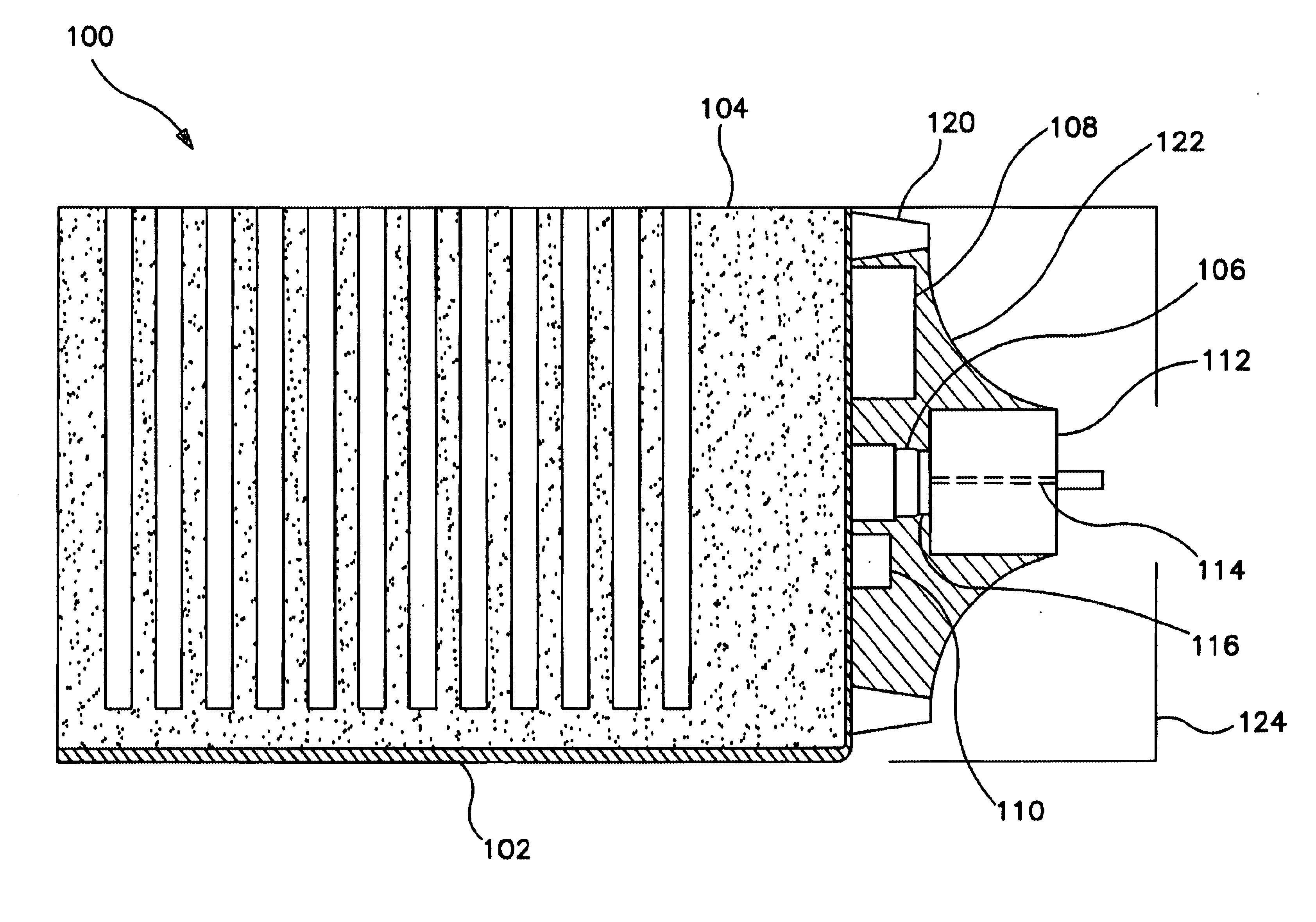
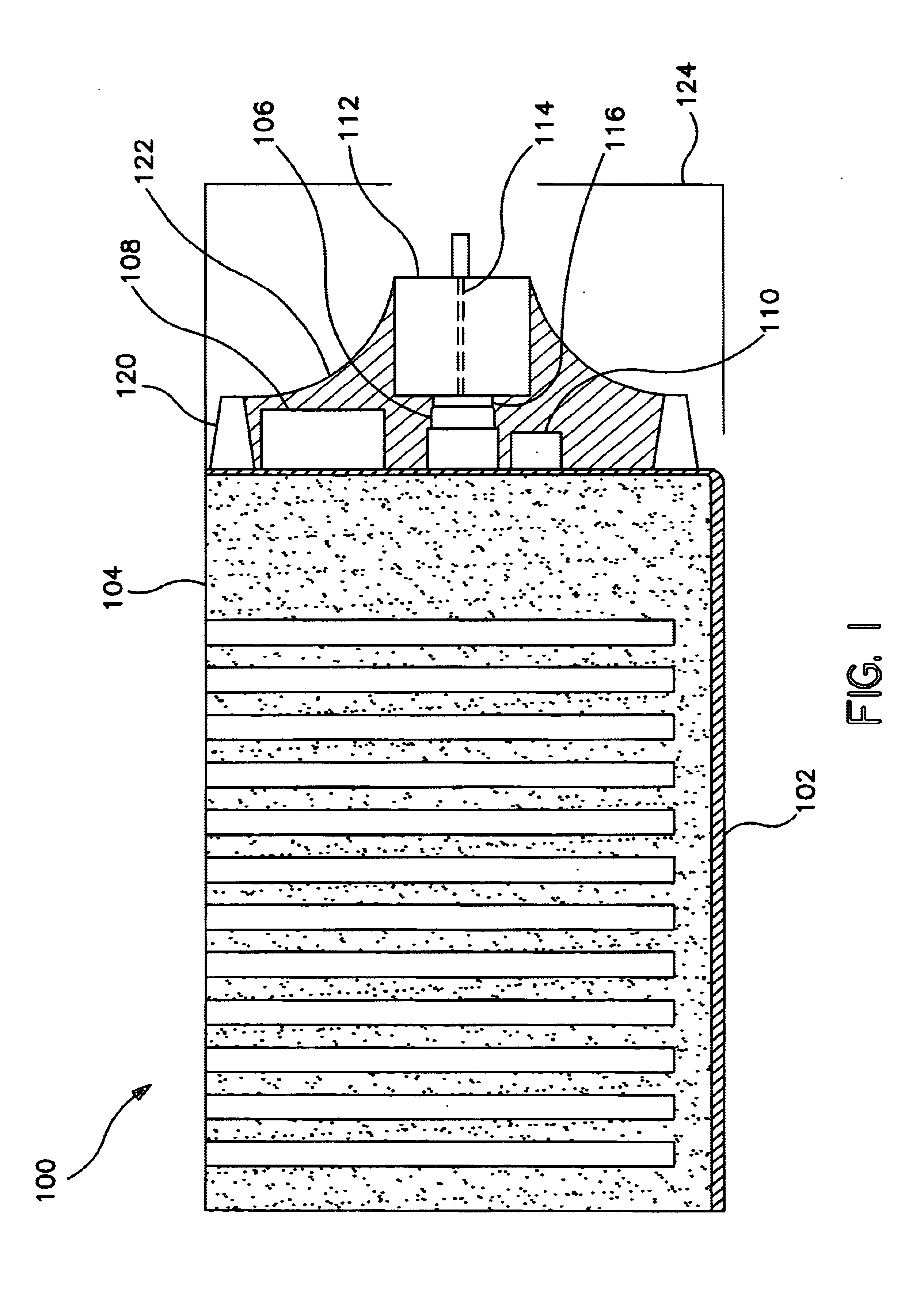
[0055]The following embodiments will be described in the context of an optical transceiver, receiver or transceiver module and a method of making the same. Those skilled in the art, however, will recognize that the disclosed methods and structures are adaptable for broader applications. If the same reference numeral is repeated with respect to different figures, it refers to the corresponding structure in each figure.
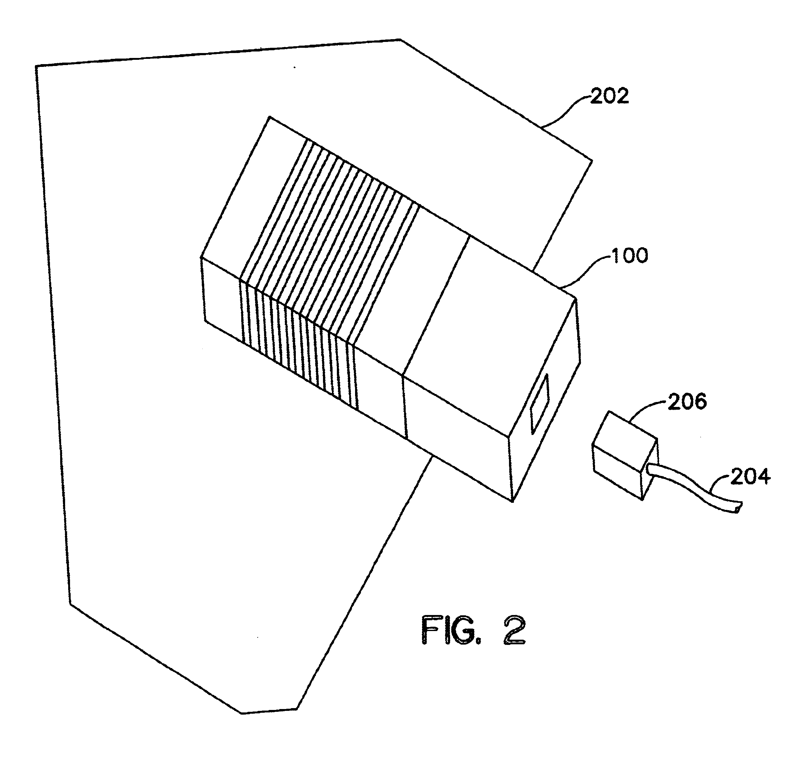
[0056]With reference to FIG. 1, an optical transmitter, receiver or transceiver module 100 is depicted, according to an embodiment of the invention. The optical module 100 comprises a flexible printed circuit board 102 that wraps around and attaches to a circuit board mounting structure 104. The flexible printed circuit board 102 functions to support the electrical components of the optical module 100, such as an array of optoelectronic devices 106, a driver or amplifier chip 108, and a photo-detector 110. A first ferrule 112, packaging an array of optica...
PUM
Abstract
A process is provided for aligning and connecting at least one optical fiber to at least one optoelectronic device so as to couple light between at least one optical fiber and at least one optoelectronic device. One embodiment of this process comprises the following steps: (1) holding at least one optical element close to at least one optoelectronic device, at least one optical element having at least a first end; (2) aligning at least one optical element with at least one optoelectronic device; (3) depositing a first non-opaque material on a first end of at least one optoelectronic device; and (4) bringing the first end of at least one optical element proximate to the first end of at least one optoelectronic device in such a manner that the first non-opaque material contacts the first end of at least one optoelectronic device and the first end of at least one optical element. The optical element may be an optical fiber, and the optoelectronic device may be a vertical cavity surface emitting laser. The first non-opaque material may be a UV optical adhesive that provides an optical path and mechanical stability. In another embodiment of the alignment process, the first end of at least one optical element is brought proximate to the first end of at least one optoelectronic device in such a manner that an interstitial space exists between the first end of at least one optoelectronic device and the first end of at least one optical element.
Description
CROSS REFERENCE TO RELATED APPLICATIONS[0001]This application is related to the following co-pending applications, each assigned to the Assignee of the present invention.[0002]application Ser. No. 09 / 749,279, filed Dec. 26, 2000, entitled “Apparatus for Holding an Optical Element”;[0003]application Ser. No. 09 / 749,281, filed Dec. 26, 2000, entitled “An Apparatus and Method of Using Flexible Printed Circuit Board in Optical Transceiver Device (as amended)”;[0004]Application Ser. No. 09 / 749,282, filed Dec. 26, 2000, entitled “Attenuator and Conditioner”;[0005]Application Ser. No. 09 / 749,283, filed Dec. 26, 2000, entitled “Optoelectronic Mounting Structure”;[0006]Application Ser. No. 09 / 749,284 filed Dec. 26, 2000, entitled “Optical Transmitter, Receiver or Transceiver Module”;[0007]Application Ser. No. 09 / 749,285 filed Dec. 26, 2000, entitled “Housing and Mounting Structure”; and[0008]Application Ser. No. 09 / 749,286, filed Dec. 26, 2000, entitled “Optical Power Control System”.FIELD O...
Claims
Application Information
Patent Timeline
Application Date:The date an application was filed.
Publication Date:The date a patent or application was officially published.
First Publication Date:The earliest publication date of a patent with the same application number.
Issue Date:Publication date of the patent grant document.
PCT Entry Date:The Entry date of PCT National Phase.
Estimated Expiry Date:The statutory expiry date of a patent right according to the Patent Law, and it is the longest term of protection that the patent right can achieve without the termination of the patent right due to other reasons(Term extension factor has been taken into account ).
Invalid Date:Actual expiry date is based on effective date or publication date of legal transaction data of invalid patent.
Inventor ANDERSON, GENE R.ARMENDARIZ, MARCELINO G.BRYAN, ROBERT P.CARSON, RICHARD F.CHU, DAHWEYDUCKETT, III, EDWIN B.GIUNTA, RACHEL KNUDSENMITCHELL, ROBERT T.MCCORMICK, FREDERICK B.PETERSON, DAVID W.RISING, MERIDETH A.REBER, CATHLEEN A.REYSEN, BILL H.