Method to fabricate high-performance NPN transistors in a BiCMOS process

Inactive Publication Date: 2005-06-14
GLOBALFOUNDRIES US INC
View PDF0 Cites 19 Cited by
  • Summary
  • Abstract
  • Description
  • Claims
  • Application Information

AI Technical Summary

Benefits of technology

[0014]One object of the present invention is to provide a simple, yet reliable

Problems solved by technology

As the vertical dimensions of the bipolar transistor are scaled more and more, serious device operational limitations have been encountered.
The ion implantation will cause damage, however, to the base region.
Such damage may ultimately lead to degradation in device performance.
The selective epitaxy with a cavity structure mandates stringent process requirements for good selectivity, and suff

Method used


Image

  • Method to fabricate high-performance NPN transistors in a BiCMOS process
  • Method to fabricate high-performance NPN transistors in a BiCMOS process
  • Method to fabricate high-performance NPN transistors in a BiCMOS process

Examples


Embodiment Construction

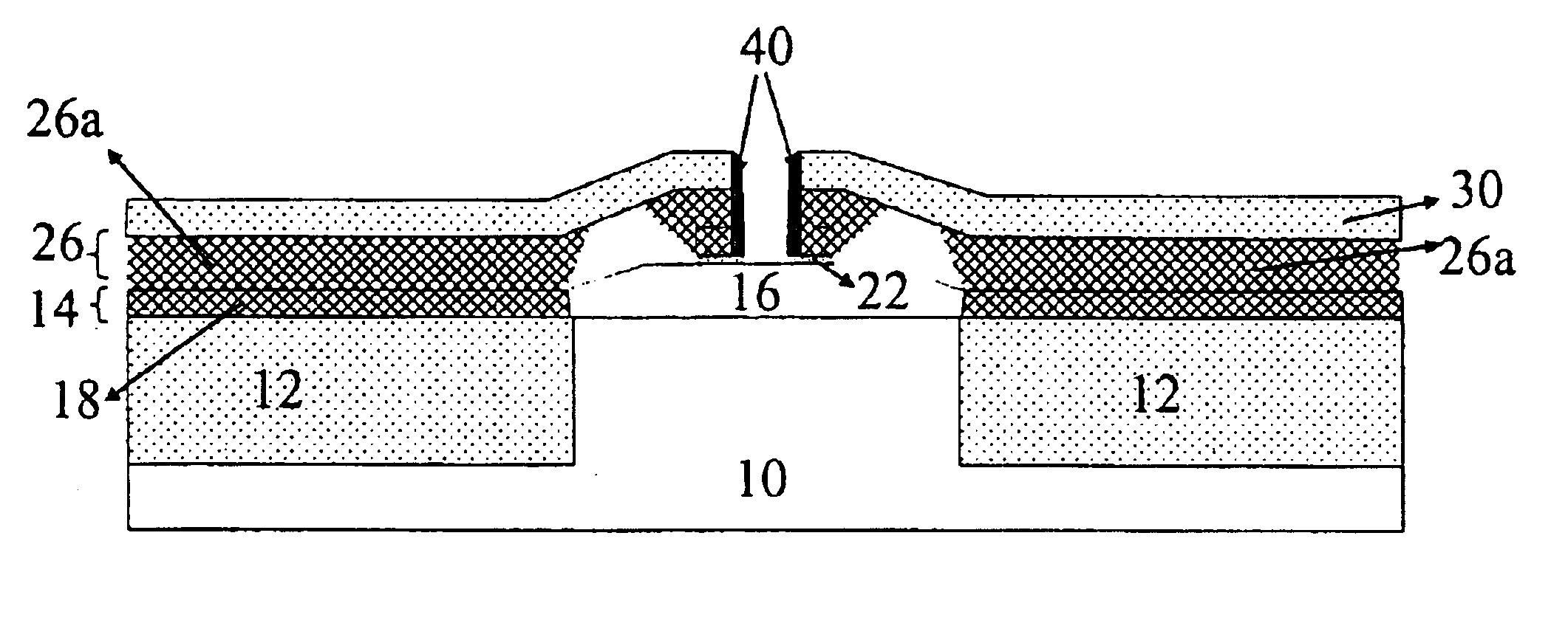
[0036]The present invention, which provides a method for fabricating a high-performance transistor in a BiCMOS process in which a patterned emitter landing pad stack is employed as well as the resultant structure that is formed from the inventive method, will now be described in greater detail by referring to the drawings that accompany the present application. The drawings of the present application are directed to the HBT device area. For clarity, the CMOS device area as well as other areas of a typically BiCMOS structure are not shown in the drawings of the present application.

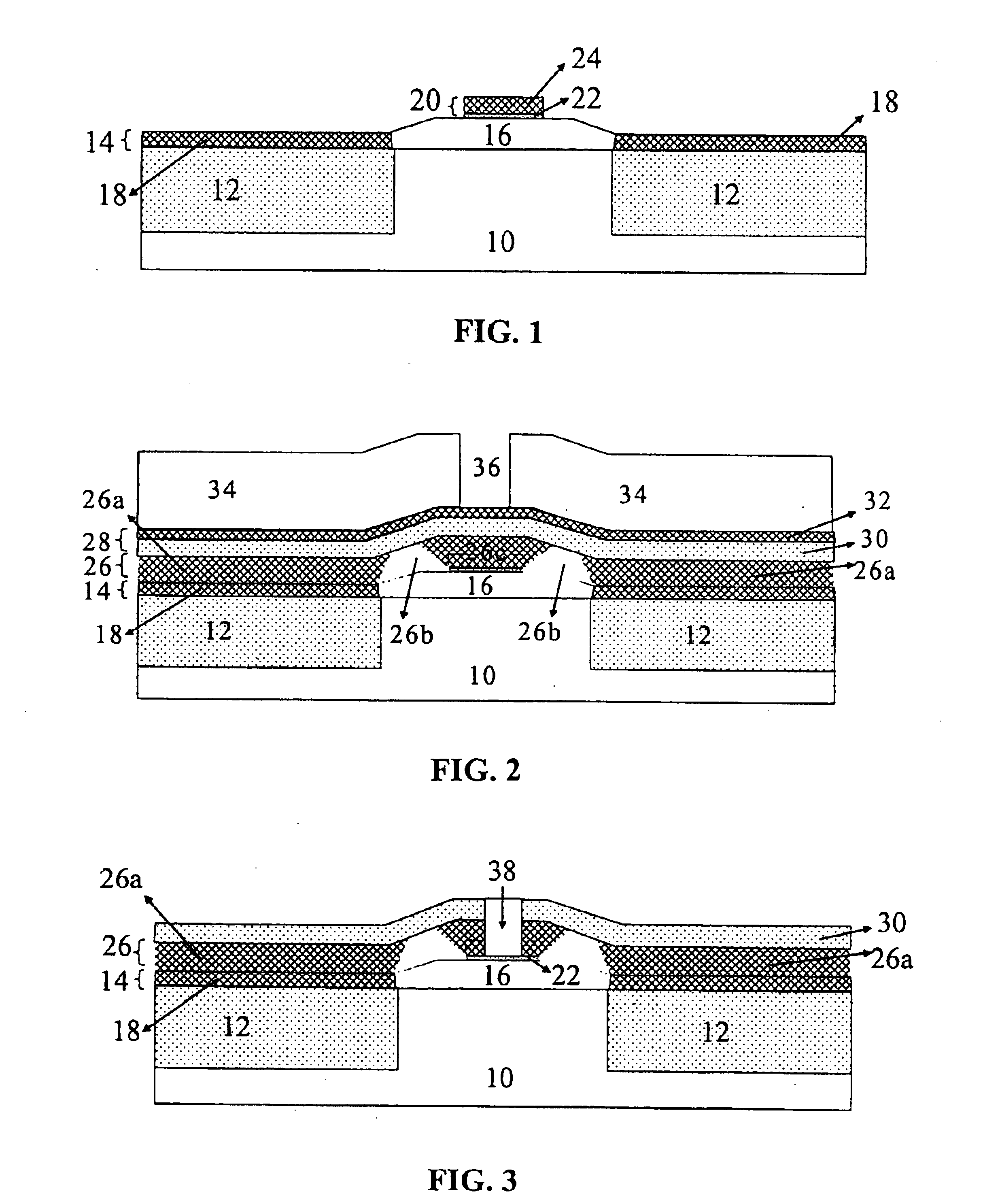
[0037]FIG. 1 shows an initial structure of the present invention. The initial structure includes a Si substrate 10 having trench isolation regions 12 formed therein. The Si substrate 10 may be a Si-containing semiconductor structure such as Si, SiGe or a silicon-on-insulator. Alternatively, the Si substrate 10 may be a Si layer such as epi-Si or a:Si formed atop of a semiconductor substrate. The Si substrat...


PUM


Abstract

A method of forming a quasi-self-aligned heterojunction bipolar transistor (HBT) that exhibits high-performance is provided. The method includes the use of a patterned emitter landing pad stack which serves to improve the alignment for the emitter-opening lithography and as an etch stop layer for the emitter opening etch. The present invention also provides an HBT that includes a raised extrinsic base having monocrystalline regions located beneath the emitter landing pad stack.

Description

RELATED APPLICATION[0001]This application is a divisional of U.S. application Ser. No. 10 / 249,821, filed May 9, 2003, U.S. Pat. No. 6,809,024.FIELD OF THE INVENTION[0002]The present invention relates generally to a bipolar transistor and, more particularly, to a method for forming a bipolar transistor with a raised extrinsic base in an integrated bipolar and complementary metal oxide semiconductor (BiCMOS) transistor circuit.BACKGROUND OF THE INVENTION[0003]Bipolar transistors are electronic devices with two p-n junctions that are in close proximity to each other. A typical bipolar transistor has three device regions: an emitter, a collector, and a base disposed between the emitter and the collector. Ideally, the two p-n junctions, i.e., the emitter-base and collector-base junctions, are in a single layer of semiconductor material separated by a specific distance. Modulation of the current flow in one p-n junction by changing the bias of the nearby junction is called “bipolar-transi...

Claims


Application Information

Patent Timeline
IPC IPC(8): H01L21/331H01L21/02H01L21/70H01L21/8249H01L29/66H01L29/737
CPCH01L21/8249H01L29/7378H01L29/66242
Inventor DUNN, JAMES S.FEILCHENFELD, NATALIE B.LIU, QIZHISTRICKER, ANDREAS D.
Owner GLOBALFOUNDRIES US INC
Why Eureka
Try Eureka