Contaminant removal by laser-accelerated fluid

a technology of laser acceleration and laser acceleration, applied in fluid pressure measurement, instruments, manufacturing tools, etc., can solve the problems of major problems such as circuit fatal defects, and the removal of particles and other contaminants from solid-state surfaces

Inactive Publication Date: 2005-06-21
APPL MATERIALS ISRAEL LTD +1
View PDF16 Cites 28 Cited by
  • Summary
  • Abstract
  • Description
  • Claims
  • Application Information

AI Technical Summary

Benefits of technology

[0008]It is an object of some aspects of the present invention to provide improve...

Problems solved by technology

Removal of particles and other contaminants from solid-state surfaces is a major problem in integrated circuit manufacture.
As the trend to miniaturize electronic devices and components conti...

Method used


Image

  • Contaminant removal by laser-accelerated fluid
  • Contaminant removal by laser-accelerated fluid
  • Contaminant removal by laser-accelerated fluid

Examples


Embodiment Construction

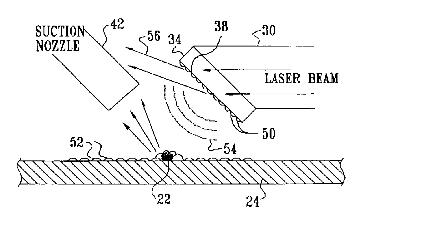
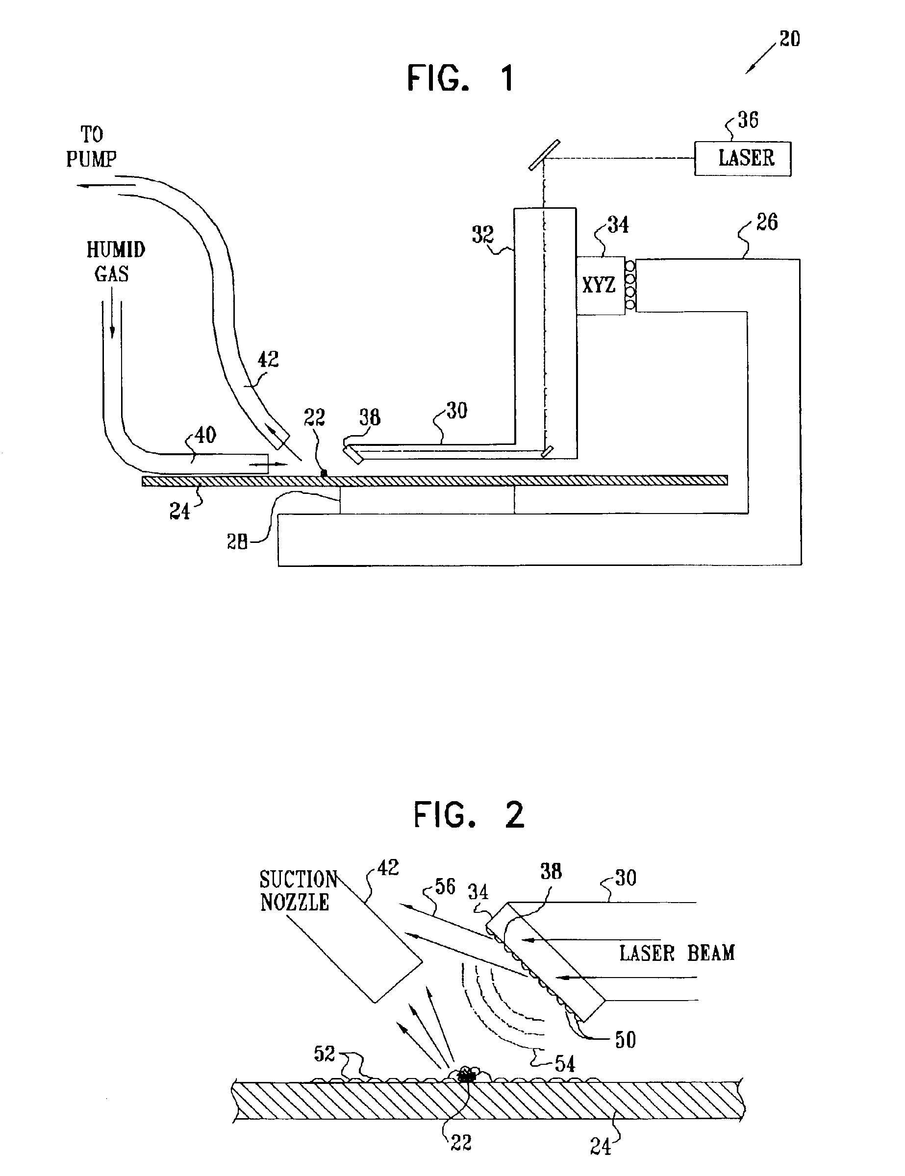
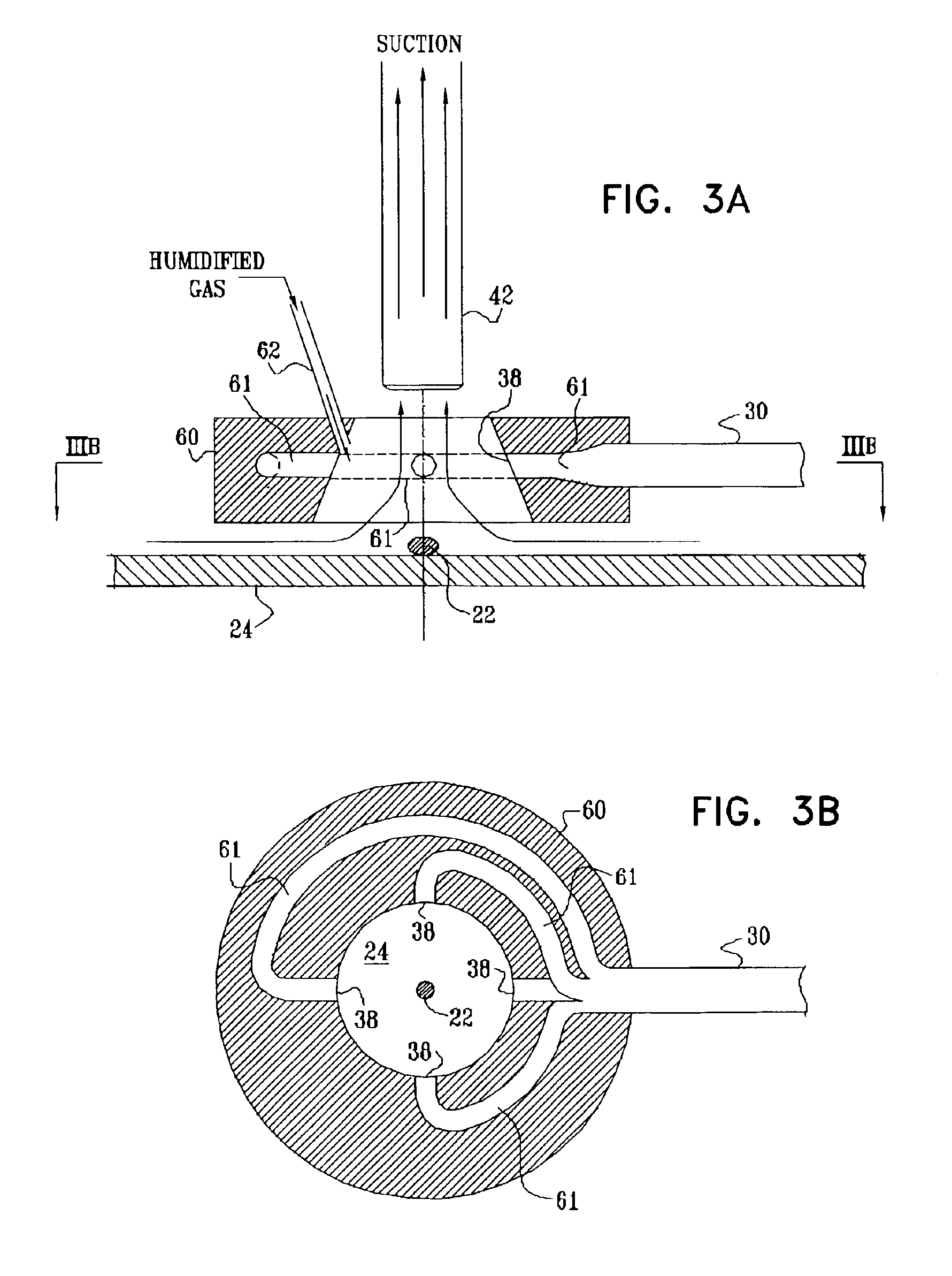
[0031]FIG. 1 is a schematic side view of a system 20 for removal of a particle 22 from a substrate 24, in accordance with a preferred embodiment of the present invention. Typically, substrate 24 comprises a semiconductor wafer, photomask or other item used in manufacturing semiconductor devices, although the methods embodied in system 20 may also be applied to cleaning substrates of other types. The substrate is supported by a chuck 28, typically a rotating chuck that is a part of a motion control system 26. The substrate and associated elements shown in FIG. 1 are typically contained in a process chamber, not shown in the figures, as is known in the art of semiconductor device manufacture.

[0032]For optimal operation of system 20, it is desirable to know the coordinates of particle 22 with high accuracy, preferably to within ±5 μm. This level of accuracy is typically provided by wafer inspection tools such as the Tencor 7200 system (KLA-Tencor, San Jose, Calif.), or the “Excite” ins...


PUM

PropertyMeasurementUnit
Pressureaaaaaaaaaa
Angleaaaaaaaaaa

Abstract

A method for removing a particle from a substrate includes forming a layer of a fluid on a surface of an optical element and positioning the optical element in proximity to a location of the particle on the substrate. A pulse of electromagnetic radiation is directed to impinge on the surface of the optical element so as to induce explosive evaporation of the fluid thereon, whereby a pressure wave is emitted toward the location of the particle.

Description

FIELD OF THE INVENTION[0001]The present invention relates generally to processing of semiconductor devices, and specifically to methods and apparatus for removal of foreign particles and other contaminants from solid-state surfaces.BACKGROUND OF THE INVENTION[0002]Removal of particles and other contaminants from solid-state surfaces is a major problem in integrated circuit manufacture. Integrated circuit manufacture includes, but is not limited to, production of semiconductor wafers, printed circuit boards, component packaging, and the like. As the trend to miniaturize electronic devices and components continues, and critical dimensions of circuit features become ever smaller, the presence of even a minute foreign particle on a wafer substrate during processing can cause a fatal defect in the circuit. Similar concerns affect other elements used in the manufacturing process, such as photomasks and reticles.[0003]Various methods are known in the art for stripping and cleaning foreign ...

Claims


Application Information

Patent Timeline
IPC IPC(8): B08B7/00B23K26/14H01L21/00H01L21/02H01L21/306
CPCB08B7/0035B08B7/0042H01L21/67051H01L21/02046B23K26/1417B23K26/146
Inventor UZIEL, YORAM
Owner APPL MATERIALS ISRAEL LTD
Why Eureka
Try Eureka