Flash memory array with increased coupling between floating and control gates

a flash memory array and control gate technology, applied in the direction of basic electric elements, electrical equipment, semiconductor devices, etc., can solve the problems of limiting the amount of shrinkage of the overall layout, the difficulty of performing both of these functions, and the limit of the layout of a given circuit, so as to increase the area of the memory cell

Inactive Publication Date: 2005-06-21
WODEN TECH INC
View PDF50 Cites 58 Cited by
  • Summary
  • Abstract
  • Description
  • Claims
  • Application Information

AI Technical Summary

Benefits of technology

[0012]According to a primary aspect of the present invention, an increased floating gate vertical surface area is provided on a projection from a base element that interfaces with the substrate surface, wherein the projection is much smaller in one direction than the base and preferably the same size as the base in the other direction. The control gate that interfaces with the vertical surfaces of the floating gate projection, with an inter-gate dielectric layer therebetween, can be positioned within the area of the floating gate base, thereby not causing the area the memory cell to be increased as a result. And the base can still be made with dimensions across the substrate surface equal to the minimum resolvable element size for the process being used.
[0013]The floating gate is shaped, according to one specific configuration, as an inverted “T”, as viewed across the length of a memory cell channel between its source and drain regions. A thin base portion of the minimum element size is positioned over the substrate with gate dielectric therebetween, and a thinner portion projects upward from the base in its middle. This projection preferably extends completely across the base in an orthogonal direction, across the width of the channel, thereby to provide a significant amount of vertical surface area for coupling with a control gate that is positioned adjacent the surfaces of the projection through an inter-gate dielectric layer. The control gate wraps over the projection but need not extend beyond the base in a direction of the length of the channel.
[0015]According to another aspect of the present invention, for a different type of memory cell that erases its floating gate to an erase gate instead of to the substrate, the floating gate is provided with a base and narrow projection as described above, except that the projection need not be made to extend very high. An erase gate wraps around the projection with a suitable tunnel dielectric therebetween. The sharp edges on the top of the projection enhance tunneling of electrons from the floating gate to the erase gate through the intermediate dielectric.

Problems solved by technology

It is often difficult to perform both of these functions in an optimum manner with a single voltage.
But there are usually limits of how far a given circuit layout can be shrunk in this manner, since there is often at least one feature that is limited as to how much it can be shrunk, thus limiting the amount that the overall layout can be shrunk.

Method used


Image

  • Flash memory array with increased coupling between floating and control gates
  • Flash memory array with increased coupling between floating and control gates
  • Flash memory array with increased coupling between floating and control gates

Examples


Embodiment Construction

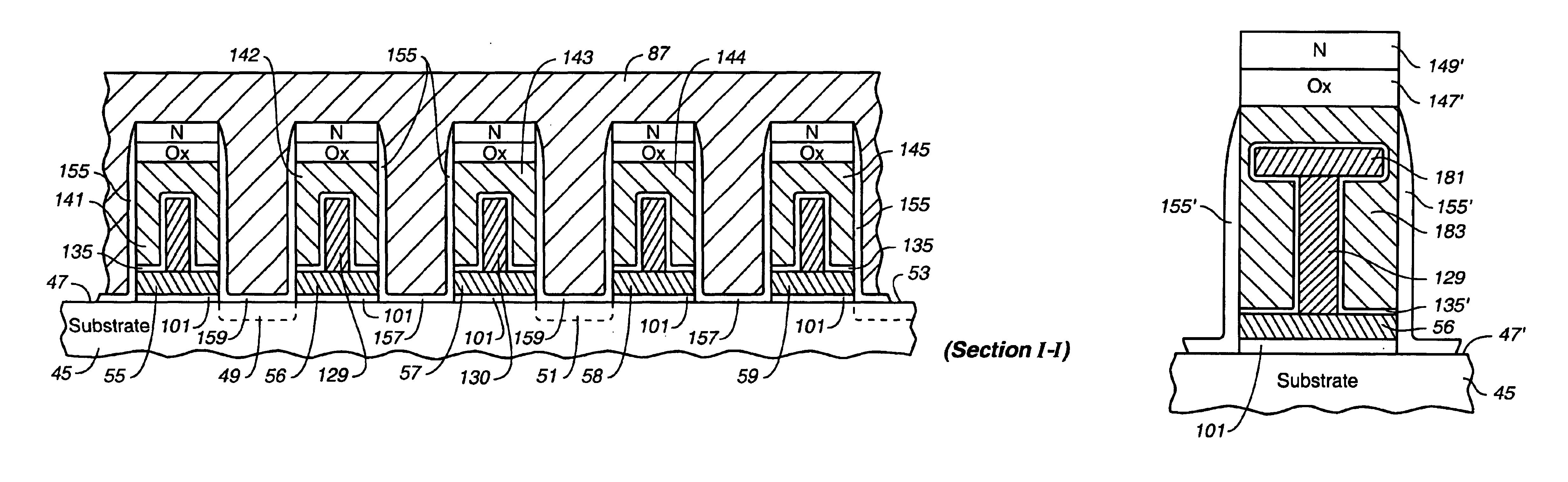
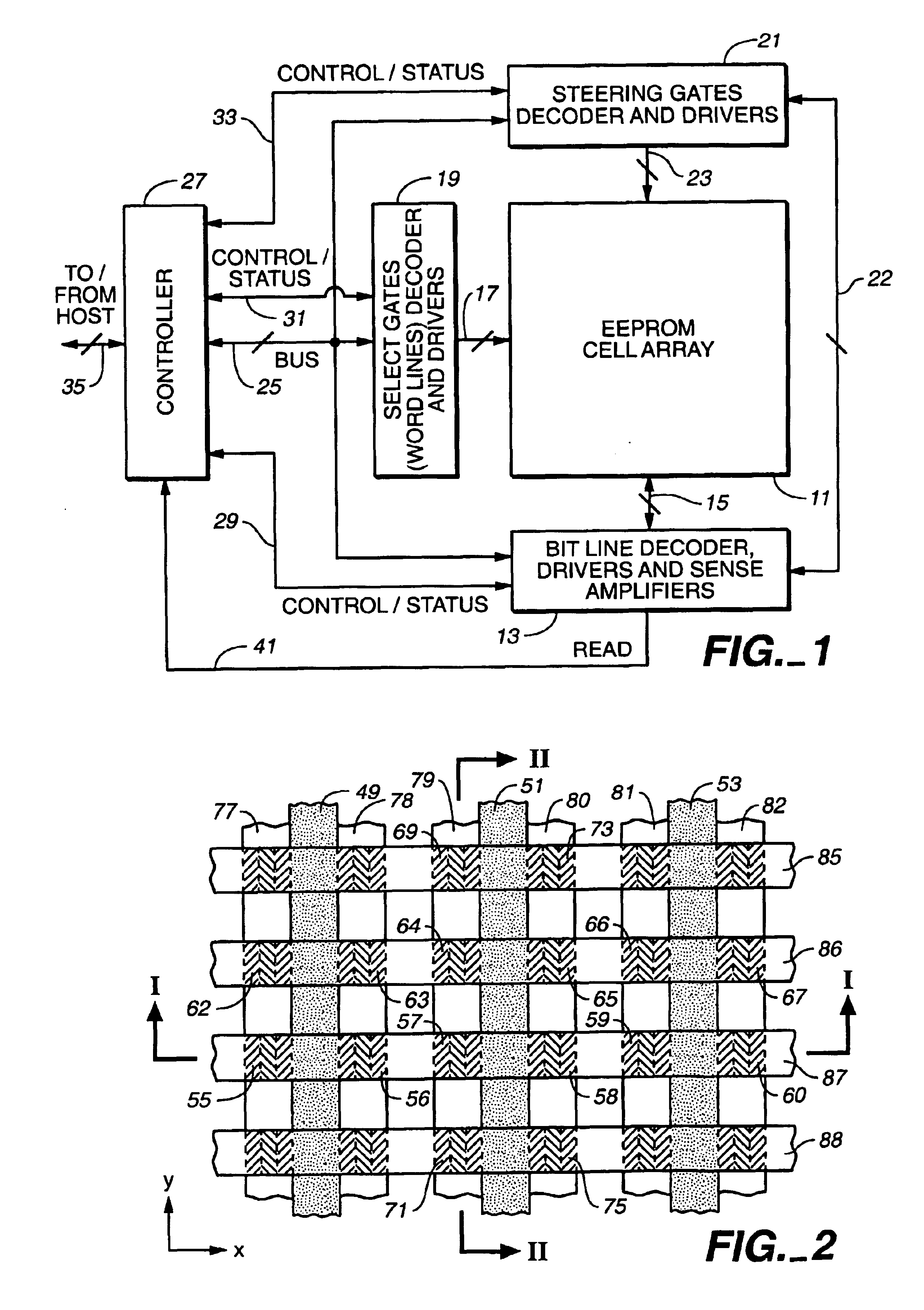
[0029]An example memory system incorporating the various aspects of the present invention is generally illustrated in the block diagram of FIG. 1. A large number of individually addressable memory cells 11 are arranged in a regular array of rows and columns, although other physical arrangements of cells are certainly possible. Bit lines, designated herein to extend along columns of the array 11 of cells, are electrically connected with a bit line decoder and driver circuit 13 through lines 15. Word lines, which are designated in this description to extend along rows of the array 11 of cells, are electrically connected through lines 17 to a word line decoder and driver circuit 19. Steering gates, which extend along columns of memory cells in the array 11, are electrically connected to a steering gate decoder and driver circuit 21 through lines 23. Each of the decoders 13, 19 and 21 receives memory cell addresses over a bus 25 from a memory controller 27. The decoder and driving circu...


PUM


Abstract

Floating gate structures are disclosed which have a base field coupled with the substrate and a narrow projection extending from the base away from the substrate. In one form, surfaces of a relatively large projection provide an increased surface area for a control gate that wraps around it, thereby increasing the coupling between the two. In another form, an erase gate wraps around a relatively small projection in order to take advantage of sharp edges of the projection to promote tunneling of electrons from the floating to the erase gate. In each case, the control or floating gate is positioned within the area of the floating gate in one direction, thereby not requiring additional substrate area for such memory cells.

Description

FIELD OF THE INVENTION[0001]This invention relates generally to non-volatile flash memory systems, and, more specifically, to the structures of memory cells and arrays of memory cells, and to the process of forming them.BACKGROUND[0002]There are many commercially successful non-volatile memory products being used today, particularly in the form of small form factor cards, which use an array of flash EEPROM (Electrically Erasable and Programmable Read Only Memory) cells having a “split-channel” between source and drain diffusions. The floating gate of the cell is positioned over one portion of the channel and the word line (also referred to as a control gate) is positioned over the other channel portion as well as over the floating gate. This effectively forms a cell with two transistors in series, one (the memory transistor) with a combination of the amount of charge on the floating gate and the voltage on the word line controlling the amount of current that can flow through its por...

Claims


Application Information

Patent Timeline
Patent Type & Authority Patents(United States)
IPC IPC(8): H01L27/115H01L21/70H01L29/423H01L29/40H01L21/8247
CPCH01L27/115H01L27/11521H01L27/11526H01L29/7881H01L29/42324H01L29/66825H01L27/11543H10B41/48H10B41/40H10B69/00H10B41/30
Inventor YUAN, JACK H.
Owner WODEN TECH INC
Why Eureka
Try Eureka