Microlens array substrate, method of manufacturing the same, and display device

a microlens array and substrate technology, applied in the field of microlens array substrate, a method of manufacturing the same, and a display device, can solve the problems of increasing costs, microlens arrays giving no attention to the improvement of contrast, and the contrast between pixels cannot be improved by conventional microlens arrays, so as to reduce the number of steps and production costs, and the effect of easy formation

Inactive Publication Date: 2005-06-21
SEIKO EPSON CORP
View PDF12 Cites 189 Cited by
  • Summary
  • Abstract
  • Description
  • Claims
  • Application Information

AI Technical Summary

Benefits of technology

[0011]According to the present invention, the substrate precursor is closely placed between the first and second master molds and the lenses are formed by transferring the shapes of the curved surfaces of the first master mold. A microlens array substrate having a plurality of lenses can be thus easily formed. Because each lens converges incident light, a display screen can be brightly illuminated. Moreover, because the first and second master molds can be used repeatedly as long as durability permits, the step of producing these master molds can be omitted in the steps of manufacturing the second and subsequent microlens array substrates, thereby reducing the number of steps and production costs.
[0012]The recesses are formed on the microlens array substrate by transferring the shapes of the projections of the second master mold, and the recesses are filled with the shading material. The shading material functions as a black matrix to improve contrast between pixels.
[0013]According to the present invention, a microlens array substrate capable of improving contrast in addition to illuminating brightly a display screen can be easily manufactured by transferring.
[0014](2) In this manufacturing method, the substrate precursor may be closely placed between the first and second master molds such that each of the projections avoids being positioned right above the center of each of the curved surfaces.

Problems solved by technology

However, these methods require a lithographic step each time when manufacturing an individual microlens array, thereby leading to increased costs.
A microlens array illuminates a display screen, but contrast between pixels is not improved by a conventional microlens array.
However, a conventional method of manufacturing a microlens array has given no attention to the improvement of contrast.

Method used


Image

  • Microlens array substrate, method of manufacturing the same, and display device
  • Microlens array substrate, method of manufacturing the same, and display device
  • Microlens array substrate, method of manufacturing the same, and display device

Examples


first embodiment

(First Embodiment)

[0063]FIGS. 1A-4B illustrate a method of manufacturing a microlens array substrate according to a first embodiment of the present invention.

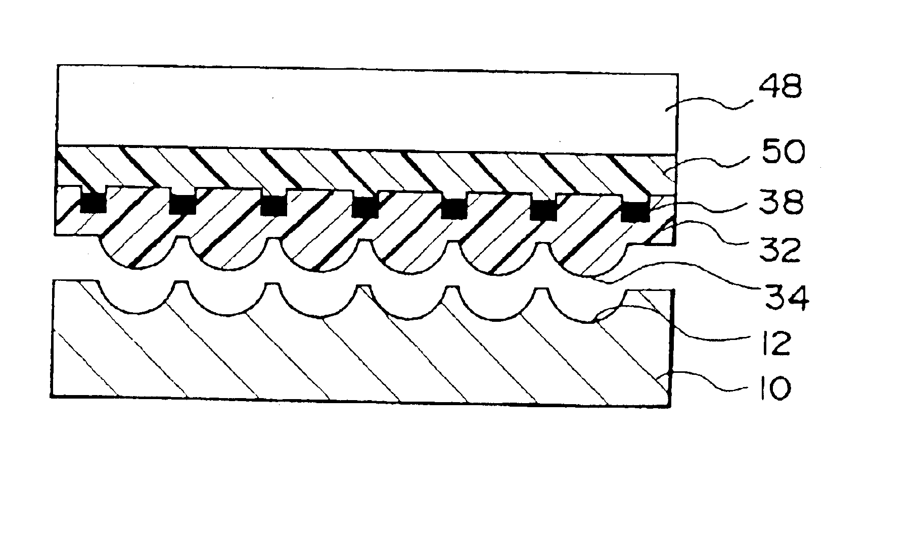
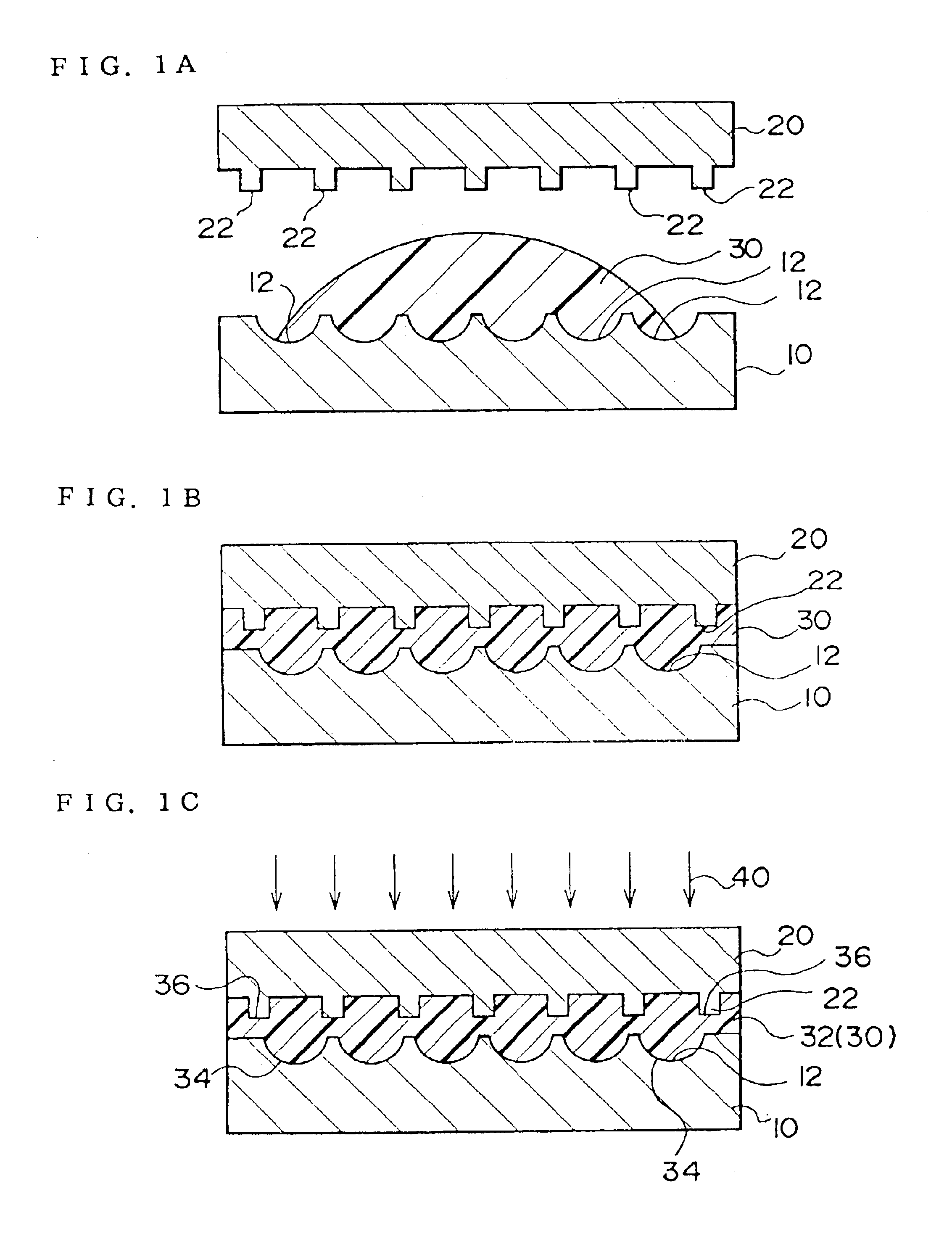
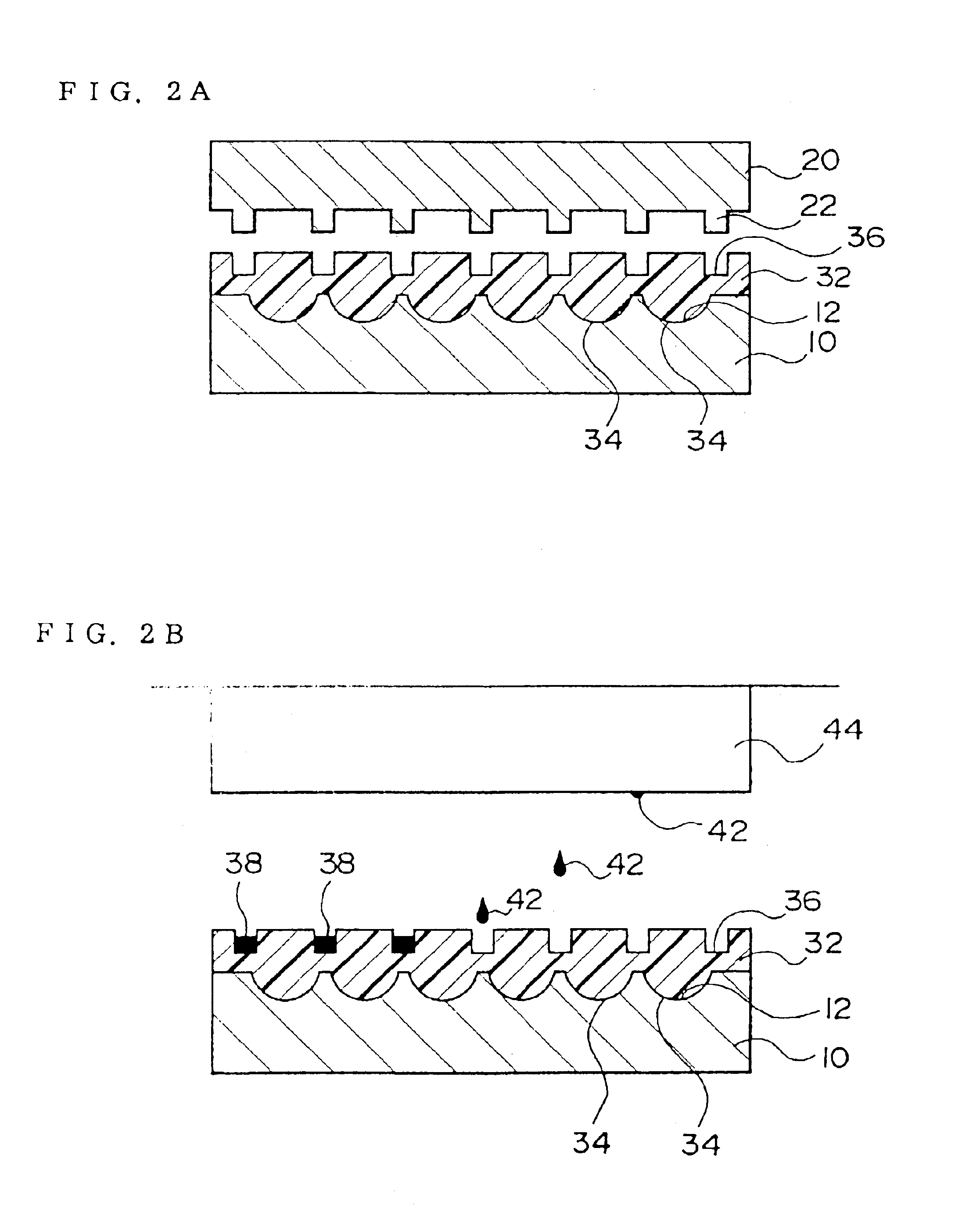
[0064]A first master mold 10 and a second master mold 20 shown in FIG. 1A are prepared. A plurality of curved surfaces 12 are formed on the first master mold 10. Each of the curved surfaces 12 has a concave shape that is an inverted shape of a convex lens. On the second master mold 20, a plurality of projections 22 are formed. These projections 22 form a black matrix as seen from a plan view (not shown).

[0065]The first and second master molds 10 and 20 are arranged such that the curved surfaces 12 face the projections 22 and each projection 22 avoids being positioned right above the center of each curved surface 12.

[0066]A substrate precursor 30 (first light transmitting layer precursor) is then closely placed between the master mold 10 and the master mold 20. The substrate precursor 30 is a material for a microlens array subst...

second embodiment

(Second Embodiment)

[0098]FIGS. 5A-6C illustrate a method of manufacturing a microlens array substrate according to a second embodiment of the present invention.

[0099]A substrate precursor 130 is closely placed between a first master mold 110 and the second master mold 20, as shown in FIG. 5A. Curved surfaces 112 are formed on the master mold 110. Each curved surface 112 has a convex shape that is an inverse of the shape of a concave lens. The present embodiment differs from the first embodiment in the shape of the curved surfaces 112. The master mold 20 is as same as in the first embodiment, and a material for the substrate precursor 130 can be selected from the materials used in the first embodiment. After the same step as in FIG. 1C, a microlens array substrate 132 is formed. Recesses 136 are formed on the microlens array substrate 132 by transferring the shapes of the projections 22 and lenses 134 are formed by transferring the shapes of the curved surfaces 112. The lenses 134 ar...

third embodiment

(Third Embodiment)

[0105]FIGS. 7-9B illustrate a method of manufacturing a microlens array substrate according to a third embodiment of the present invention. In the present embodiment, a microlens array substrate 200 shown in FIG. 7 is manufactured. The microlens array substrate 200 differs from the microlens array substrate 32 shown in FIG. 2B in the shape of recesses 202. Specifically, each recess 202 has a tapered side. Because the opening of the recess 202 is wider than the bottom, it can be reliably filled with the shading material 42 (see FIG. 2B) even if the pixels are densely arranged. A master mold with projections each having a trapezoid cross section is used to form the recesses 202.

[0106]FIGS. 8A-9B illustrate a process of forming a master mold used for forming the recesses 202.

[0107]A resist layer 214 is formed on a base 212, as shown in FIG. 8A. The base 212 is formed into a master mold by etching the surface thereof. Although there are no specific limitations to the m...


PUM

PropertyMeasurementUnit
wavelengthaaaaaaaaaa
thicknessaaaaaaaaaa
thicknessaaaaaaaaaa

Abstract

A method of manufacturing a microlens array substrate is provided comprising the steps of: closely providing a substrate precursor (30) between a first master mold (10) having a plurality of curved surfaces (12) and a second master mold (20) having a plurality of projections (22) to form a substrate (32) having a plurality of lenses (34) formed by the curved surfaces (12) and recesses (36) formed by the projections (22); removing the first and second master molds (10, 20) from the substrate (32); and filling the recesses (36) with a shading material (42) after the second master mold (20) is removed.

Description

TECHNICAL FIELD[0001]The present invention relates to a microlens array substrate, a method of manufacturing the same, and a display device.BACKGROUND ART[0002]A microlens array formed by a number of micro lenses arranged side by side has been applied to liquid crystal panels, for example. Each lens of the microlens array converges incident light upon each pixel to illuminate a display screen.[0003]As a method of manufacturing a microlens array, methods using dry etching or wet etching have been known. However, these methods require a lithographic step each time when manufacturing an individual microlens array, thereby leading to increased costs.[0004]Therefore, a method of manufacturing a microlens array by dripping a liquid resin onto a master mold having curved surfaces corresponding to lenses and removing the solidified resin has been developed as disclosed in Japanese Patent Application Laid-Open No. 3-198003.[0005]A microlens array illuminates a display screen, but contrast be...

Claims


Application Information

Patent Timeline
Patent Type & Authority Patents(United States)
IPC IPC(8): G02B3/00G09F9/00B29D11/00
CPCG02B3/0031
Inventor NISHIKAWA, TAKAO
Owner SEIKO EPSON CORP
Why Eureka
Try Eureka