Multi-height FinFETS

a technology of finfets and fins, applied in the field of field effect transistors, can solve the problems of short channel effect, short channel effect, current leakage, and always critical issues in manufacturing reliability and cost, and achieve the effect of optimizing height ratio and high channel width granularity without sacrificing yield

Inactive Publication Date: 2005-06-21
AURIGA INNOVATIONS INC
View PDF11 Cites 172 Cited by
  • Summary
  • Abstract
  • Description
  • Claims
  • Application Information

AI Technical Summary

Benefits of technology

[0016]Therefore, as shown above, the invention allows FinFET devices to be tuned according to a circuit designer's needs through the use of multiple fins that can have different heights. Further, t...

Problems solved by technology

Indeed, the very large scale integration (“VLSI”) devices, having more than 100,000 devices on a chip, are generally considered old technology.
In addition to performance characteristics, performance reliability, and durability of the device, the manufacturing reliability and cost are always critical issues.
Several problems arise with the miniaturization of devices, incl...

Method used


Image

  • Multi-height FinFETS
  • Multi-height FinFETS
  • Multi-height FinFETS

Examples


Embodiment Construction

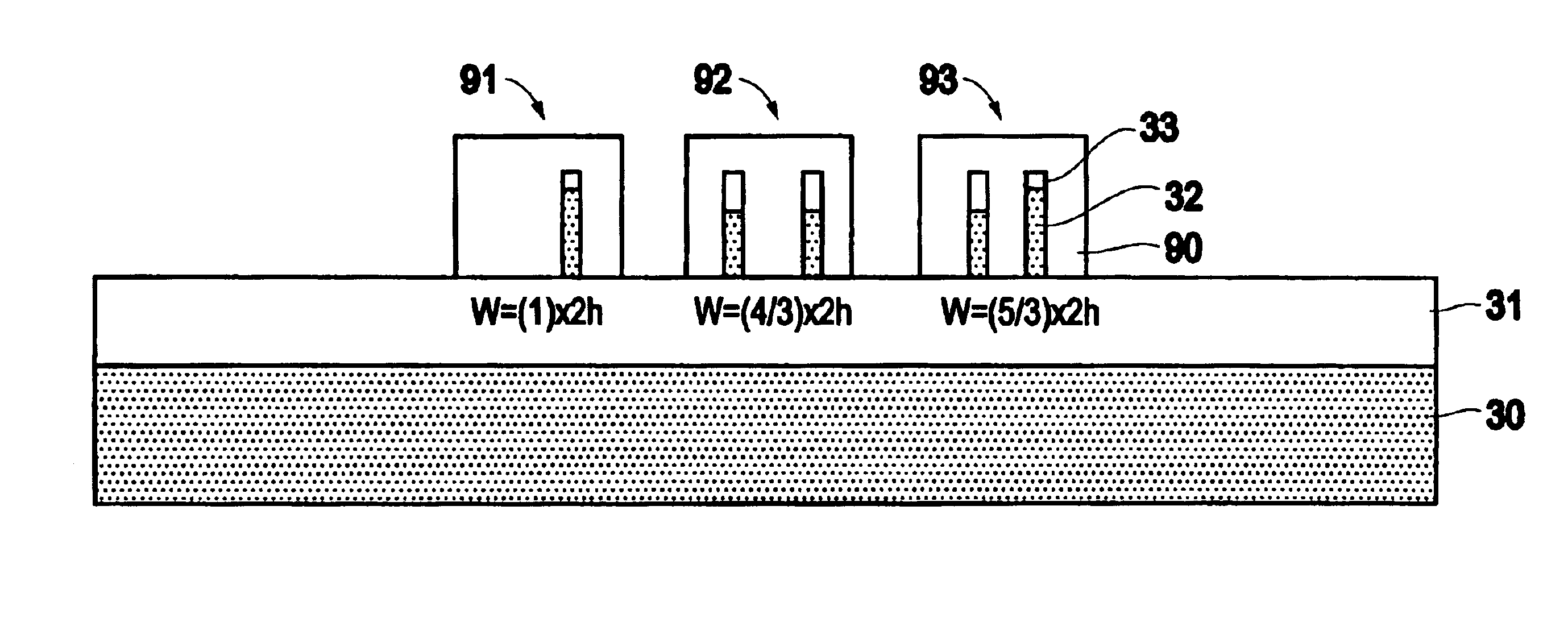
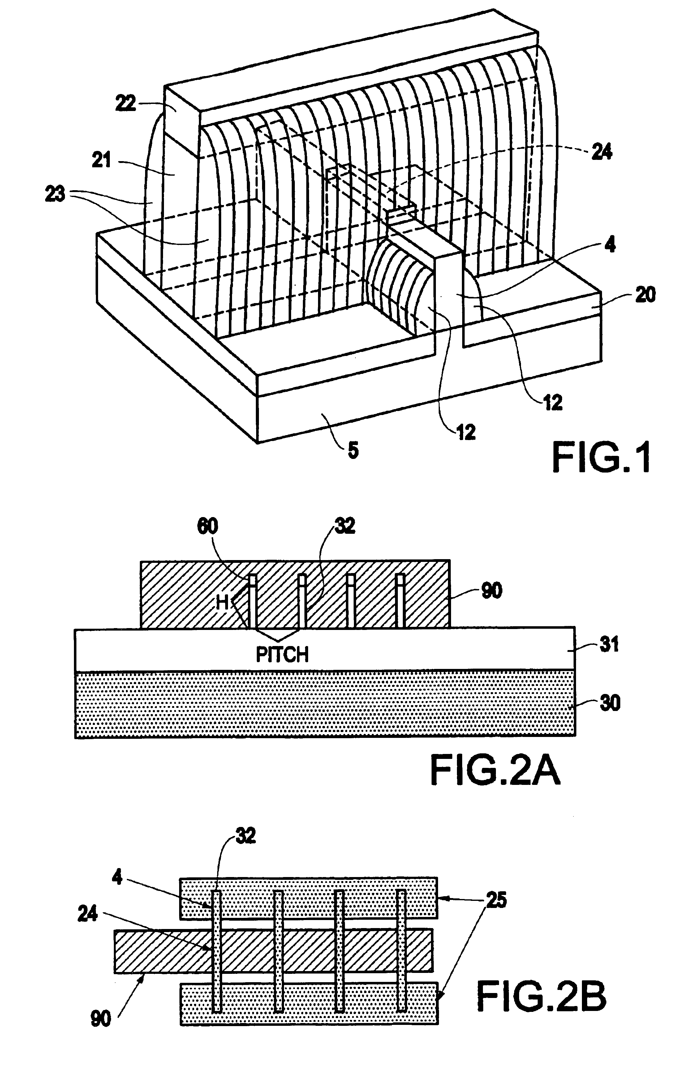
[0028]A class of analog-like circuits, in logic, such as sense-amplifiers, latches, and SRAM cells, are quite sensitive to transistor channel widths, and in particular, to ratios of channel widths of the different FETs contained within the devices. Therefore, the performance of different circuits within a chip can be tuned by altering the channel width of one or more of the FETs within the device. This permits the designer to alter the performance of the different logic circuits where necessary on the chip.

[0029]With FinFET structures, the channel width is proportional to the fin height because, in FinFET devices, the channel width is vertical. The channel width is actually twice the area created by the fin height (multiplied by the fin length) because both sides of the fin are exposed to, but insulated from the gate. Therefore, by increasing or decreasing the fin height (for a given fin length) the channel width (channel surface area exposed to, but insulated from the gate) is corr...


PUM


Abstract

The present invention provides a FinFET device that has a first fin and a second fin. Each fin has a channel region and source and drain regions that extend from the channel region. The fins have different heights. The invention has a gate conductor positioned adjacent the fins. The gate conductor runs perpendicular to the fins and crosses the channel region of each of the first fin and second fin. The fins are parallel to one another. The ratio of the height of the first fin to the height of the second fin comprises a ratio of one to 2/3. The ratio is used to tune the performance of the transistor and determines the total channel width of the transistor.

Description

BACKGROUND OF THE INVENTION[0001]1. Field of the Invention[0002]The invention relates to field effect transistors and more particularly to fin field effect transistors and to such structures that have different height fins.[0003]2. Description of Related Art[0004]Since 1960 when integrated circuits (“ICs”) were first created and fabricated, the number and density of the devices being formed on IC substrates has tremendously. Indeed, the very large scale integration (“VLSI”) devices, having more than 100,000 devices on a chip, are generally considered old technology. The fabrication of ICs having hundreds of millions of devices on a chip is standard in the market today. The development of ICs with billions of devices on each chip is under current development. Therefore, the current description of IC fabrication is ultra large scale integration (“ULSI”).[0005]As part of the increase in the number of devices formed on an IC substrate and the concurrent increase in density of the device...

Claims


Application Information

Patent Timeline
IPC IPC(8): H01L21/336H01L29/786H01L21/02H01L29/66H01L27/12H01L21/84H01L29/04
CPCH01L21/84H01L27/1203H01L29/785H01L29/66795H01L29/045H01L21/18
Inventor ALLER, INGOKEINERT, JOACHIMLUDWIG, THOMASNOWAK, EDWARD J.RAINEY, BETHANN
Owner AURIGA INNOVATIONS INC
Why Eureka
Try Eureka