
Mixed signal integrated circuit with improved isolation

a mixed signal and integrated circuit technology, applied in the direction of semiconductor devices, electrical apparatus, transistors, etc., can solve the problems of significantly attenuating the noise generated by the digital circuit section, reducing etc., to reduce the effective lateral resistance of the isolation buried layer, improve isolation, and reduce the lateral resistance of the buried layer

Inactive Publication Date: 2005-06-21
BELL SEMICON LLC +1
View PDF14 Cites 8 Cited by
  • Summary
  • Abstract
  • Description
  • Claims
  • Application Information

AI Technical Summary

Benefits of technology

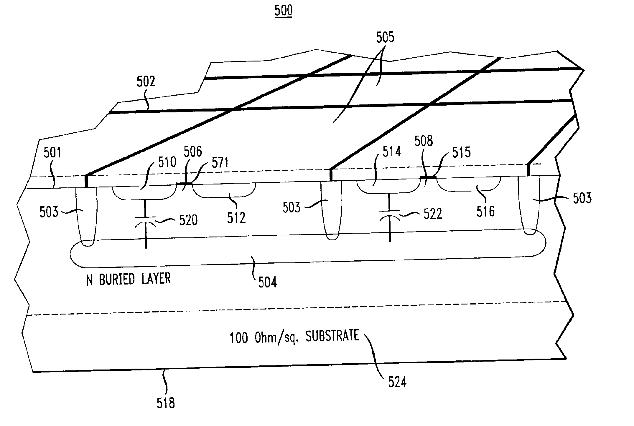
"The present invention provides techniques for improving isolation in a mixed signal integrated circuit (IC) or other device, particularly in an RF frequency range of operation. This is achieved by reducing the effective lateral resistance of an isolation buried layer formed under at least a portion of the digital circuit section of the IC. This is achieved by forming a conductive layer on an upper surface of the IC, preferably in the form of a conductive net coincident with at least a portion of the digital circuit section. The conductive layer collects noise signals generated primarily by the digital circuitry on the surface of the IC and shunts them to ground or to another reference source to which the conductive layer is connected. This reduces the noise coupling to sensitive analog circuitry and increases the electrical isolation between the digital and analog circuit sections. The invention also provides a method for reducing the effective lateral resistance of a buried layer in an IC."

Problems solved by technology

The conductive layer reduces an effective lateral resistance of the isolation buried layer, whereby an electrical isolation between the digital and analog circuit sections is increased, thus significantly attenuating noise generated by the digital circuit section.

Method used


Image

  • Mixed signal integrated circuit with improved isolation
  • Mixed signal integrated circuit with improved isolation
  • Mixed signal integrated circuit with improved isolation

Examples


Embodiment Construction

[0024]The present invention will be described herein in the context of illustrative mixed-signal integrated circuit (IC) devices. It should be appreciated, however, that the present invention is not limited to these or any other particular semiconductor device structures. Rather, the invention is more generally applicable to any semiconductor device in which it is desirable to reduce an effective lateral resistance of a buried layer by employing a conductive layer formed on a surface of the device. Furthermore, for simplification purposes only, one or more conventional semiconductor fabrication layers (e.g., p-type well, epitaxial layer, etc.) may not be shown in the several figures, but it is to be appreciated that these additional fabrication layers, where required, are nonetheless present in the IC device, as will be understood by those skilled in the art.

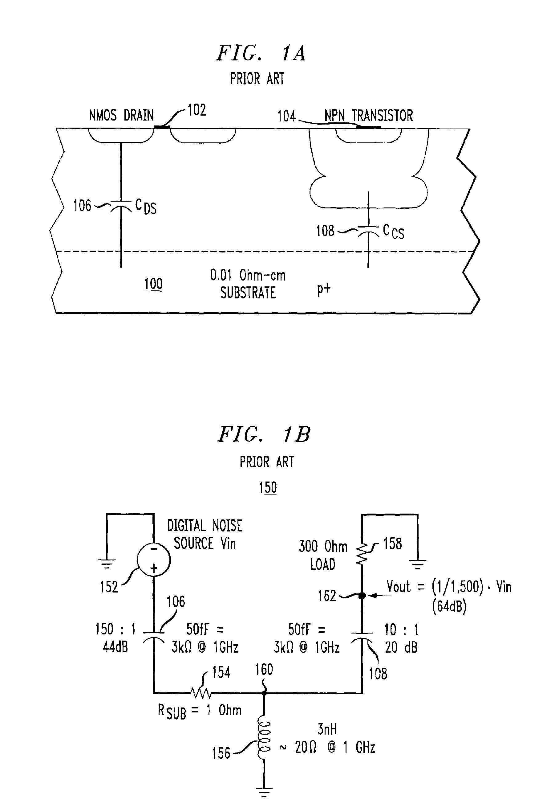
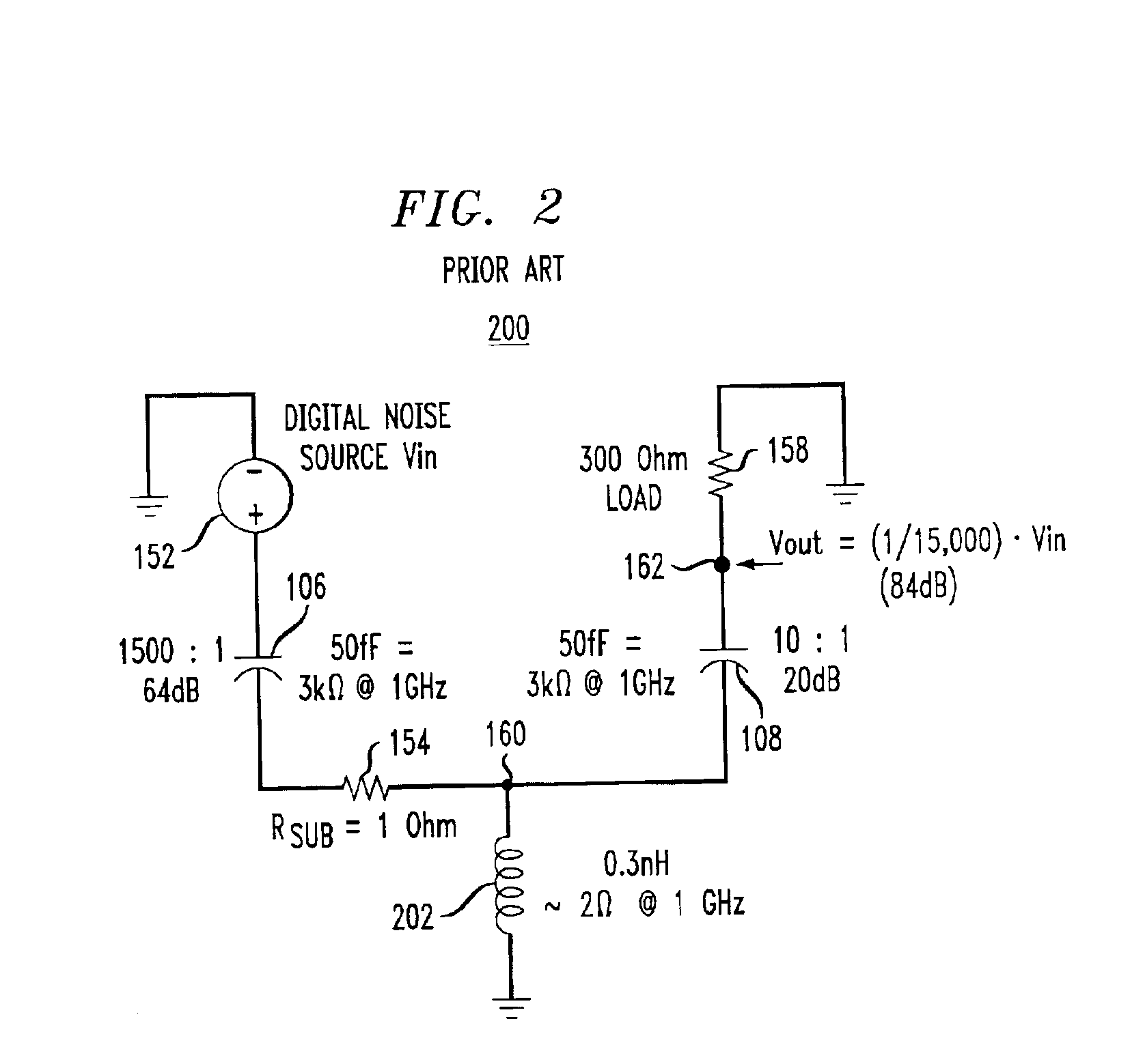
[0025]FIG. 1A depicts a vertical cross sectional view of a conventional mixed signal IC having a relatively low resistance sub...


PUM


Abstract

An integrated circuit having improved isolation includes a first circuit section formed in a substrate and a second circuit section formed in the substrate, the second circuit section being spaced laterally from the first circuit section. The integrated circuit further includes an isolation buried layer formed under at least a portion of the first circuit section, and a conductive layer formed on a surface of the substrate and electrically coupled to the buried layer and to a voltage reference, the conductive layer reducing an effective lateral resistance of the buried layer, whereby an isolation between the first and second circuit sections is increased. A second isolation buried layer can be formed under at least a portion of the second circuit section as well to provide further isolation between the first and second circuit sections.

Description

FIELD OF THE INVENTION[0001]The present invention relates generally to mixed signal integrated circuit (IC) devices, and more particularly relates to techniques for improving isolation in a mixed signal IC device by reducing a resistance of a buried layer in the IC device.BACKGROUND OF THE INVENTION[0002]Mixed signal integrated circuits (ICs) provide both analog and digital circuitry on a common substrate. For example, a mixed signal IC may include one or more sensitive radio frequency (RF) analog circuits, such as a mixer, voltage-controlled oscillator (VCO) and low-noise amplifier (LNA), as well as one or more digital logic circuits, such as a digital signal processor (DSP) or frequency synthesizer. These RF circuits generally operate at frequencies of 1 Gigahertz (GHz) and above. One of the disadvantages inherent in conventional mixed signal ICs is the problem of isolating sensitive analog circuitry from the digital circuitry, which typically generates more noise, particularly in...

Claims


Application Information

Patent Timeline
Patent Type & Authority Patents(United States)
IPC IPC(8): H01L21/70H01L21/761H01L21/8249H01L27/06
CPCH01L21/761H01L27/0623H01L21/8249
Inventor DAVIS, PAUL C.
Owner BELL SEMICON LLC
Learn More