Hybrid planar and finFET CMOS devices

Inactive Publication Date: 2005-06-28
AURIGA INNOVATIONS INC
View PDF14 Cites 110 Cited by
  • Summary
  • Abstract
  • Description
  • Claims
  • Application Information

AI Technical Summary

Benefits of technology

[0011]Another object of the present invention is to provide a simple, yet easy method for providing hybrid planar and FinFET CMOS devices.
[0012]These and other objects and advantages are achieved in the present invention by a method in which resist imaging and a patterned hard mask are used in trimming the width of the FinFET active device region and subsequent resist imaging and etching are used in thinning the thickness of the FET device area. The tri

Problems solved by technology

To compensate for this discrepancy, pFETs are typically designed with larger widths in order to balance pull-up currents against the nFET pull-down currents and achieve uniform circuit switching; nFETs with larger widths are undesirable since they take up a significant amount of chip a

Method used


Image

  • Hybrid planar and finFET CMOS devices
  • Hybrid planar and finFET CMOS devices
  • Hybrid planar and finFET CMOS devices

Examples


Embodiment Construction

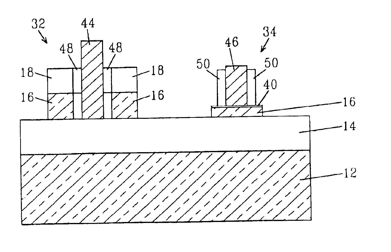
[0036]The present invention, which provides hybrid planar and FinFET CMOS devices and a method of forming the same, will now be described in greater detail by referring to the drawings that accompany the present application. In the accompanying drawings, like and corresponding elements are referred to by like reference numerals. It should be noted that in the following description and drawings, a single nFET and a single pFinFET are shown. Although illustration is provided for a single nFET and a single pFinFET, the present invention works equally well for forming a plurality of each type of device on the SOI substrate. Additionally, the structures may be fabricated such that the vertical device is an nFinFET and the planar device is a pFET.

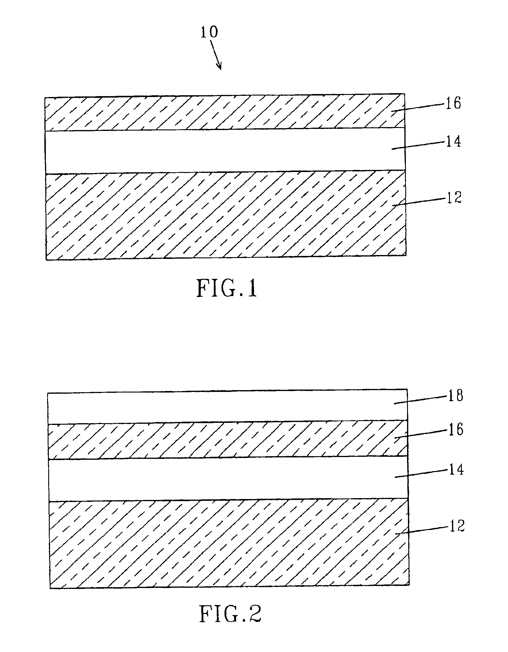
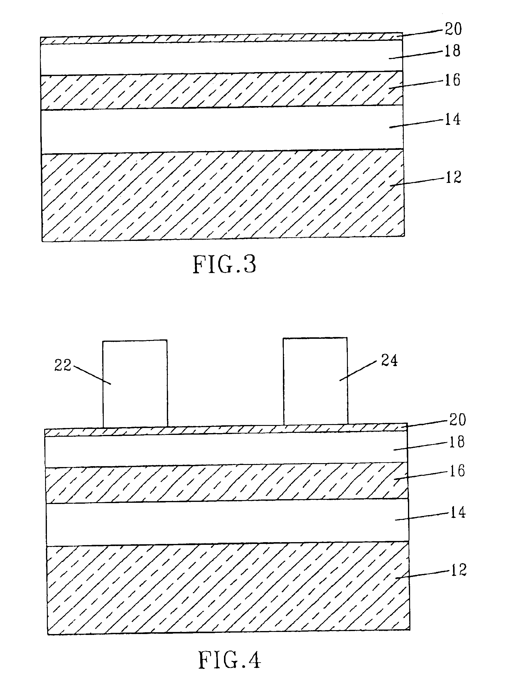
[0037]FIG. 1 illustrates an initial silicon-on-insulator (SOI) substrate 10 that may be used in the present invention. SOI substrate 10 includes a buried insulating region 14 that is positioned between a bottom semiconductor layer 12 and a top se...


PUM


Abstract

The present invention provides an integrated semiconductor circuit containing a planar single gated FET and a FinFET located on the same SOI substrate. Specifically, the integrated semiconductor circuit includes a FinFET and a planar single gated FET located atop a buried insulating layer of an silicon-on-insulator substrate, the planar single gated FET is located on a surface of a patterned top semiconductor layer of the silicon-on-insulator substrate and the FinFET has a vertical channel that is perpendicular to the planar single gated FET. A method of forming a method such an integrated circuit is also provided. In the method, resist imaging and a patterned hard mask are used in trimming the width of the FinFET active device region and subsequent resist imaging and etching are used in thinning the thickness of the FET device area. The trimmed active FinFET device region is formed such that it lies perpendicular to the thinned planar single gated FET device region.

Description

BACKGROUND OF INVENTION[0001]The present invention relates to integrated semiconductor devices, and more particularly to an integrated semiconductor circuit that includes a planar single gate complementary metal oxide semiconductor (CMOS) device and a double gate device, i.e., FinFET, which are fabricated on the same semiconductor substrate. In one instance, the planar single gate CMOS device is an nFET formed on a thin silicon-on-insulator (SOI) layer and the FinFET is a pFinFET structure having a vertical channel that has a surface orientation at the (110) direction. Alternatively, the planar single gate CMOS device is a pFET formed on a thin SOI layer with a (110) surface orientation and the FinFET is an nFinFET structure having a vertical channel that has a surface (100) orientation. The present invention also provides a method for fabricating the integrated semiconductor circuit of the present invention.[0002]In present semiconductor technology, complementary metal oxide semico...

Claims


Application Information

Patent Timeline
IPC IPC(8): H01L21/336H01L29/786H01L21/02H01L21/70H01L21/84H01L29/66H01L27/12H01L29/423H01L21/8234H01L27/08H01L27/088H01L29/49
CPCH01L21/845H01L27/1211H01L29/785H01L29/66795
Inventor DORIS, BRUCE B.BOYD, DIANE C.IEONG, MEIKEIKANARSKY, THOMAS S.KEDZIERSKI, JAKUB T.YANG, MIN
Owner AURIGA INNOVATIONS INC
Why Eureka
Try Eureka