Power-rail ESD clamp circuits with well-triggered PMOS

Inactive Publication Date: 2005-06-28
TAIWAN SEMICON MFG CO LTD
View PDF11 Cites 49 Cited by
  • Summary
  • Abstract
  • Description
  • Claims
  • Application Information

AI Technical Summary

Benefits of technology

[0023]Another objective of the invention is to provide an ESD pulse detection circuit that triggers the well of a PMOS device for efficient turn-on of the ESD clamp circuit under conditions of ESD overstress.
[0024]Yet another objective of the invention is to provide an ESD pulse detection circuit that efficiently triggers the lateral p-n-p parasitic junction transistor and the vertical p-n-p parasitic junction transistor under conditions of ESD overstress.
[0025]A further objective of the invention is to provide an ESD protection circuit that is connected between two terminals of an integrated circuit in order to dissipate an electrostatic charge from an ESD source that is placed in contact with the two terminals thereby preventing damage to the integrated circuit of to which the two terminals are connected.
[0026]Yet another objective of the invention is to provide a method for effectively protecting against ESD overstress between power rails.
[0027]The present invention provides for a new power-rail ESD clamp circuit with a well-triggered PMOS device. The method of the invention efficiently bypasses the

Problems solved by technology

In deep submicron CMOS technology, ESD damage has become one of the main reliability concerns.
Processing techniques that are applied in advanced CMOS technology procedures can lead to degradation of the performance of ESD c

Method used


Image

  • Power-rail ESD clamp circuits with well-triggered PMOS
  • Power-rail ESD clamp circuits with well-triggered PMOS
  • Power-rail ESD clamp circuits with well-triggered PMOS

Examples


Embodiment Construction

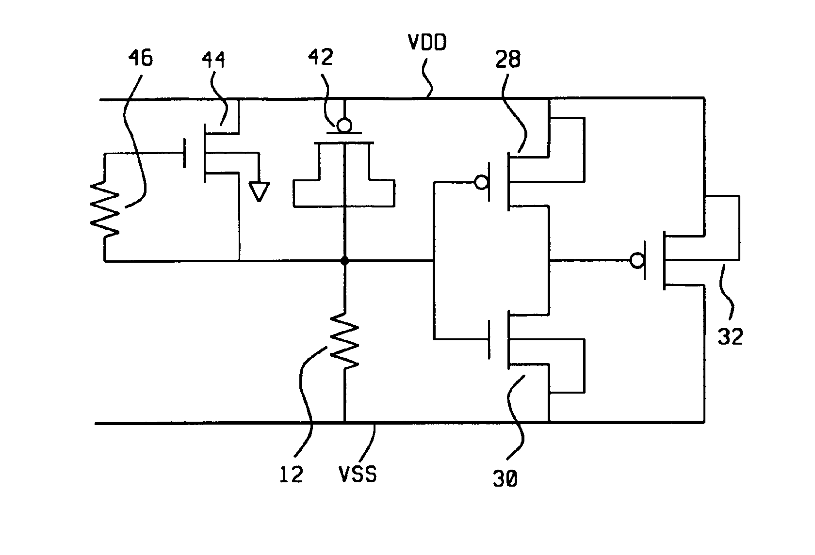
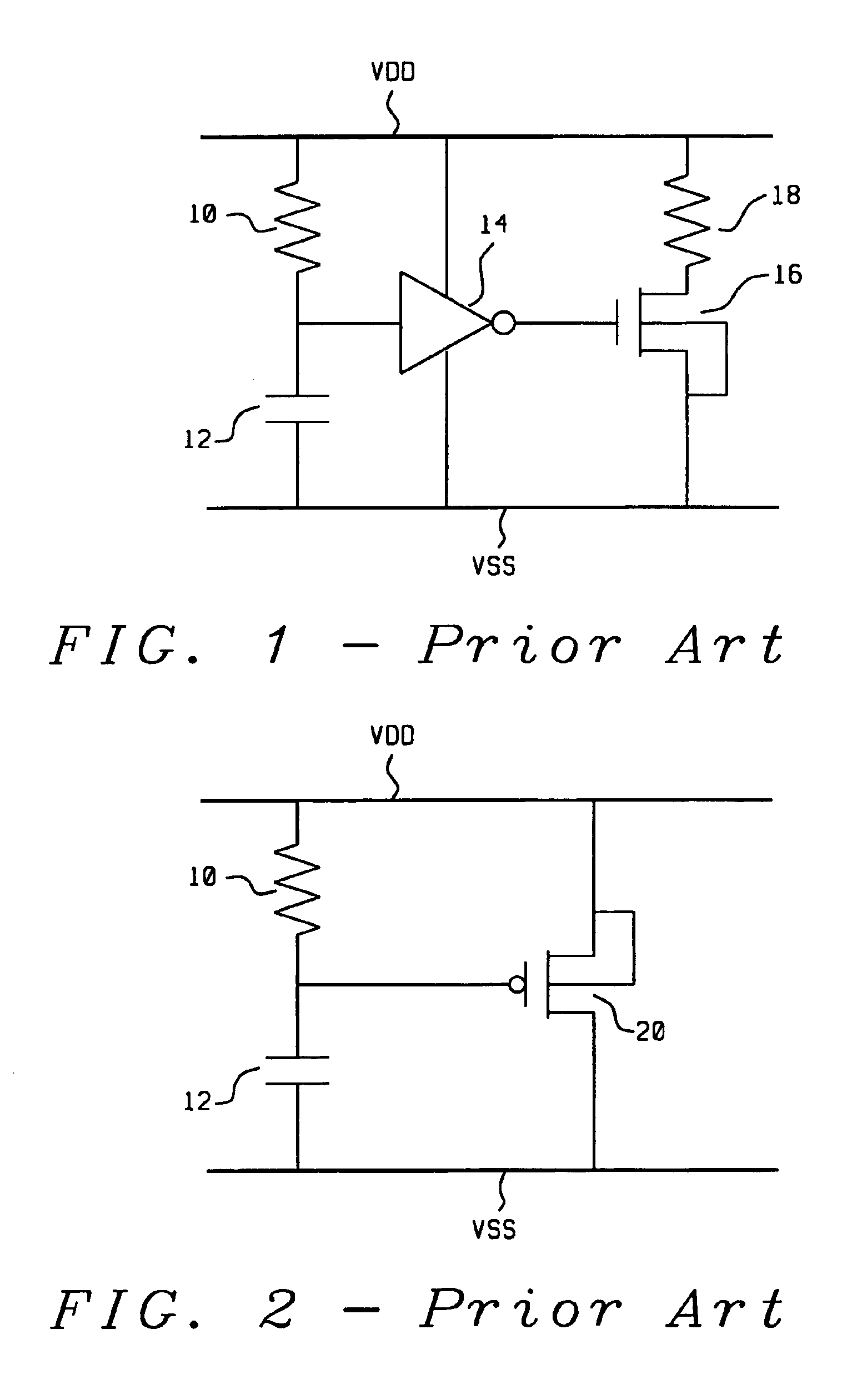
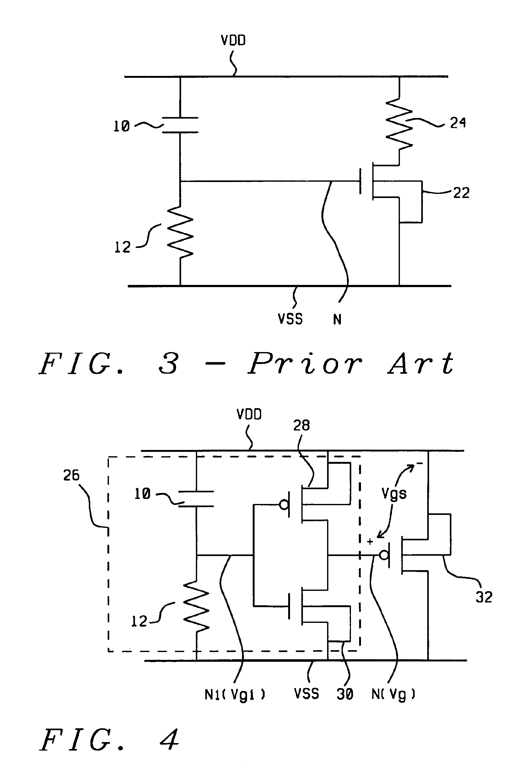
[0058]The following basic points and aspects that relate to the design of ESD protection circuits deserve to be highlighted:[0059]ESD protection circuits contain two separate functions, that is the function of detecting the presence of an ESD condition and the function of preventing an existing ESD condition from affecting the IC to which ESD protection circuit is dedicated. The first of these two functions is performed by an ESD Detection Circuit, the second function is performed by an ESD Clamp Circuit[0060]the ESD detection circuit provides a voltage at the time that an ESD condition exists, this voltage is used to drive or activate the ESD clamp circuit[0061]the existence of an ESD condition is monitored on a point of input to an IC, the existence of the ESD condition is monitored with respect to either a low voltage reference point of a ground point. This leads to two points of reference that are normally used for the evaluation of the present of an ESD condition, these two poi...


PUM


Abstract

A new ESD (Electrostatic Discharge) protection circuit with well-triggered PMOS is provided for application in power-rail ESD protection. A PMOS device is connected between the VDD and VSS power lines to sustain the ESD overstress current during the time that the ESD voltage is applied between the VDD and the VSS power lines. In deep submicron CMOS p-substrate technology, the weak point of ESD overstress control is typically associated with the NMOS device. For this reason, the invention uses a power-rail ESD clamp circuit that incorporates a PMOS device. Applying gate-coupled and N-well triggering techniques, the PMOS can be turned on more efficiently when the ESD overstress is present between the power lines. For p-substrate CMOS technology, it is difficult to couple a high voltage to the substrate of the NMOS device while high voltage is readily coupled to the N-well of a PMOS device. The proposed ESD clamp circuit can be applied efficiently to protect the ESD overstress between power rails.

Description

RELATED PATENT APPLICATION[0001]This application is related to Ser. No. 09 / 378,948 filed on Aug. 23, 1999, assigned to a common assignee.BACKGROUND OF THE INVENTION[0002](1) Field of the Invention[0003]The invention relates to the fabrication of integrated circuit devices, and more particularly, to a method for creating an Electrostatic Discharge (ESD) protection circuit for well-triggered PMOS devices.[0004](2) Description of the Prior Art[0005]In deep submicron CMOS technology, ESD damage has become one of the main reliability concerns. Processing techniques that are applied in advanced CMOS technology procedures can lead to degradation of the performance of ESD circuits that are part of Integrated Circuits (IC's). Examples of these advanced processing techniques are the formation of Lightly Doped Drain (LDD) regions in the MOSFET devices, the formation of salicided drain / source surface regions for MOSFET devices and the formation of extremely thin gate oxide layers underneath the...

Claims


Application Information

Patent Timeline
IPC IPC(8): H02H9/00H01L27/02
CPCH01L27/0266
Inventor KER, MING-DOUWU, MAU-LIN
Owner TAIWAN SEMICON MFG CO LTD
Why Eureka
Try Eureka