Versatile system for charge dissipation in the formation of semiconductor device structures

a semiconductor device and charge dissipation technology, applied in the field of semiconductor devices, can solve the problems of further compounding problems, damage to or destruction of the structure, etc., and achieve the effects of effective dissipation of charge accumulated, simple yet effective, and improved overall process yield and device reliability

Active Publication Date: 2006-09-28
TEXAS INSTR INC
View PDF8 Cites 0 Cited by
  • Summary
  • Abstract
  • Description
  • Claims
  • Application Information

AI Technical Summary

Benefits of technology

[0010] The present invention provides a versatile system, comprising a number of apparatus and methods, for effectively dissipating charge accumulated within certain semiconductor device structures during device fabrication. Comprehending various complications caused by antenna-like capacitive charging between certain conductive semiconductor structures, the system of the present invention obviates damage to surrounding structures caused by uncontrolled dissipation of that charge. The present invention provides simple yet effective alternate dissipation paths for accumulated charge—improving overall process yield and device reliability in an easy and cost-effective manner.
[0011] The present invention recognizes that electrical charge is induced in certain conductive semiconductor structures or layers (e.g., polysilicon, metal) during a number of fabrication processes (e.g., deposition, implant, plasma etch). Often that charge accumulates within a particular structure or layer, having no means to dissipate. This problem may be further compounded as more processing is performed to refine or add additional structures or layers. Under certain conditions, those additional structures or layers may accumulate additional charge that couples to and increases the charge already present. This accumulated charge pursues a path to ground (e.g., the substrate) in order to dissipate. Becoming significant enough to overcome certain thresholds or limits, the accumulated charge may discharge or dissipate to ground through an adjacent structure (e.g., gate oxide), causing damage to or destroying that structure. The present invention recognizes that the convenient and efficient provision of one or more alternate ground paths for such conductive structures obviates such concerns and problems with minimal impact on fabrication time or costs.
[0012] The present invention provides a convenient and efficient system that grounds conductive structures or layers of concern to a ground plane or layer (e.g., the semiconductor substrate), in a manner that does not impact device design or layout. The system of the present invention may be easily and efficiently implemented in a wide variety of commercial fabrication process. The present invention provides for the formation of a void or ablation through one or more intermediate layers to a ground plane or layer, prior to the formation or deposition of a conductive layer or structure of concern. As the conductive structure or layer is formed or deposited, it couples directly to the ground plane through the void. Depending upon the fabrication processes used, one or more voids may be formed along the perimeter of a particular die, or along the periphery of an entire wafer. The voids may be formed by a number of procedures or processes, and the number of voids may be varied to ensure proper coupling of the conductive layer to the ground plane.
[0013] More specifically, embodiments of the present invention provide structures and methods for dissipating any aberrant charge that may accumulate during the fabrication of a semiconductor device segment, obviating overstress or break down damage to a focal device structure that might otherwise result from uncontrolled dissipation of the aberrant charge. A substrate has first and second intermediate structures disposed atop the substrate, with the focal structure disposed atop the substrate therebetween. A first conductive structure is disposed atop the second intermediate structure, the focal structure, and a portion of the first intermediate structure. A third intermediate structure is disposed contiguously atop the first conductive structure and the first intermediate layer. A void is formed in a peripheral region of, or location along, the device segment, through the first and third intermediate layers down to the substrate. A second conductive structure is disposed atop the third intermediate structure, such that it couples the substrate through the void.

Problems solved by technology

This problem may be further compounded as more processing is performed to refine or add additional structures or layers.
Becoming significant enough to overcome certain thresholds or limits, the accumulated charge may discharge or dissipate to ground through an adjacent structure (e.g., gate oxide), causing damage to or destroying that structure.

Method used


Image

  • Versatile system for charge dissipation in the formation of semiconductor device structures
  • Versatile system for charge dissipation in the formation of semiconductor device structures
  • Versatile system for charge dissipation in the formation of semiconductor device structures

Examples


Embodiment Construction

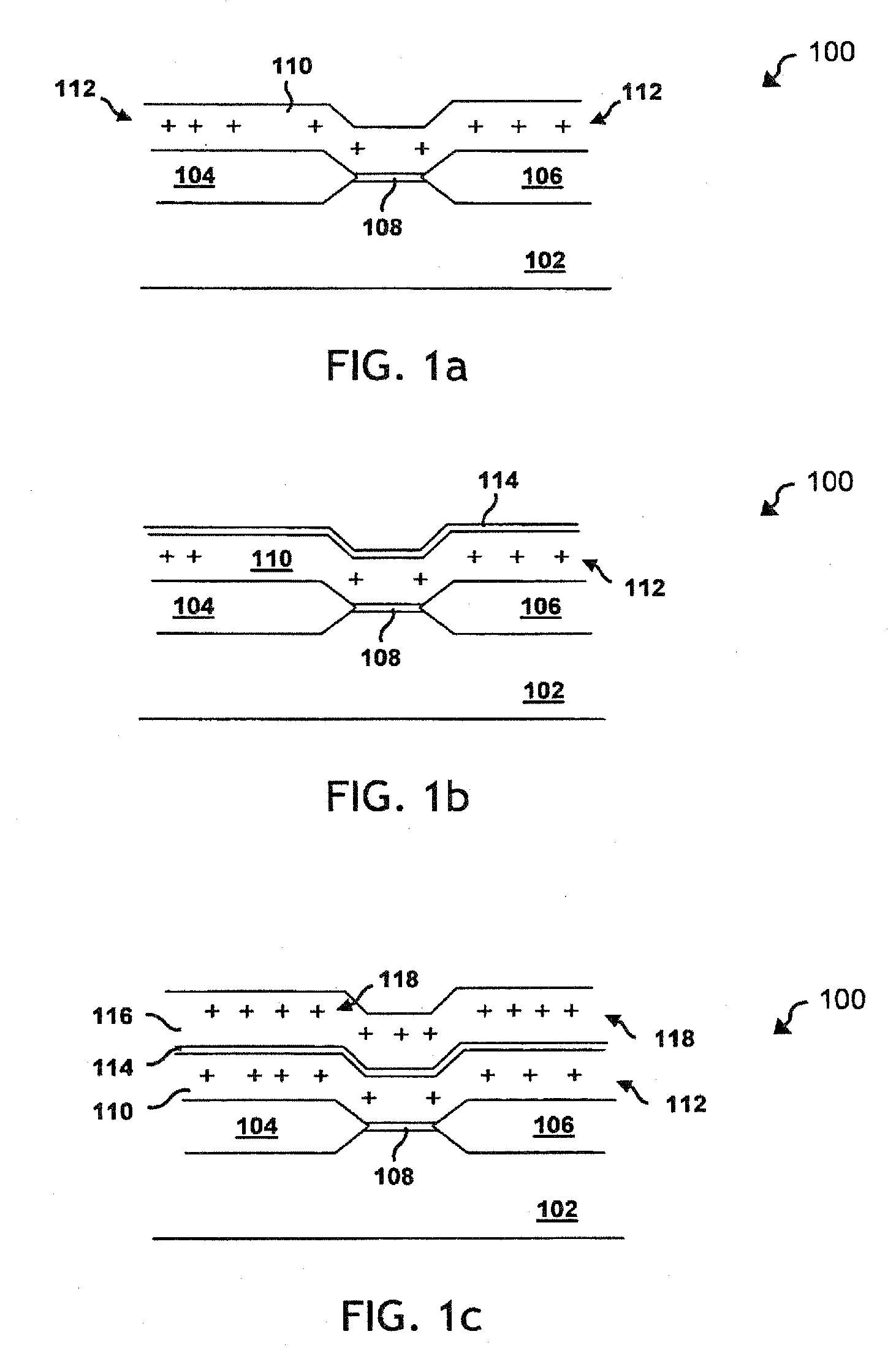
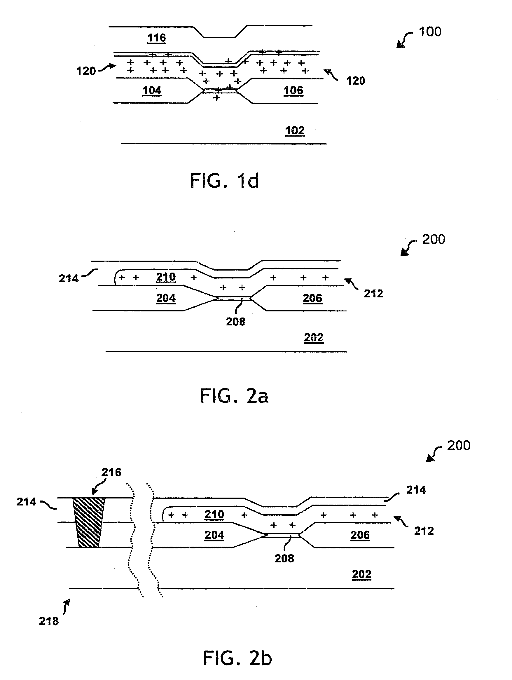
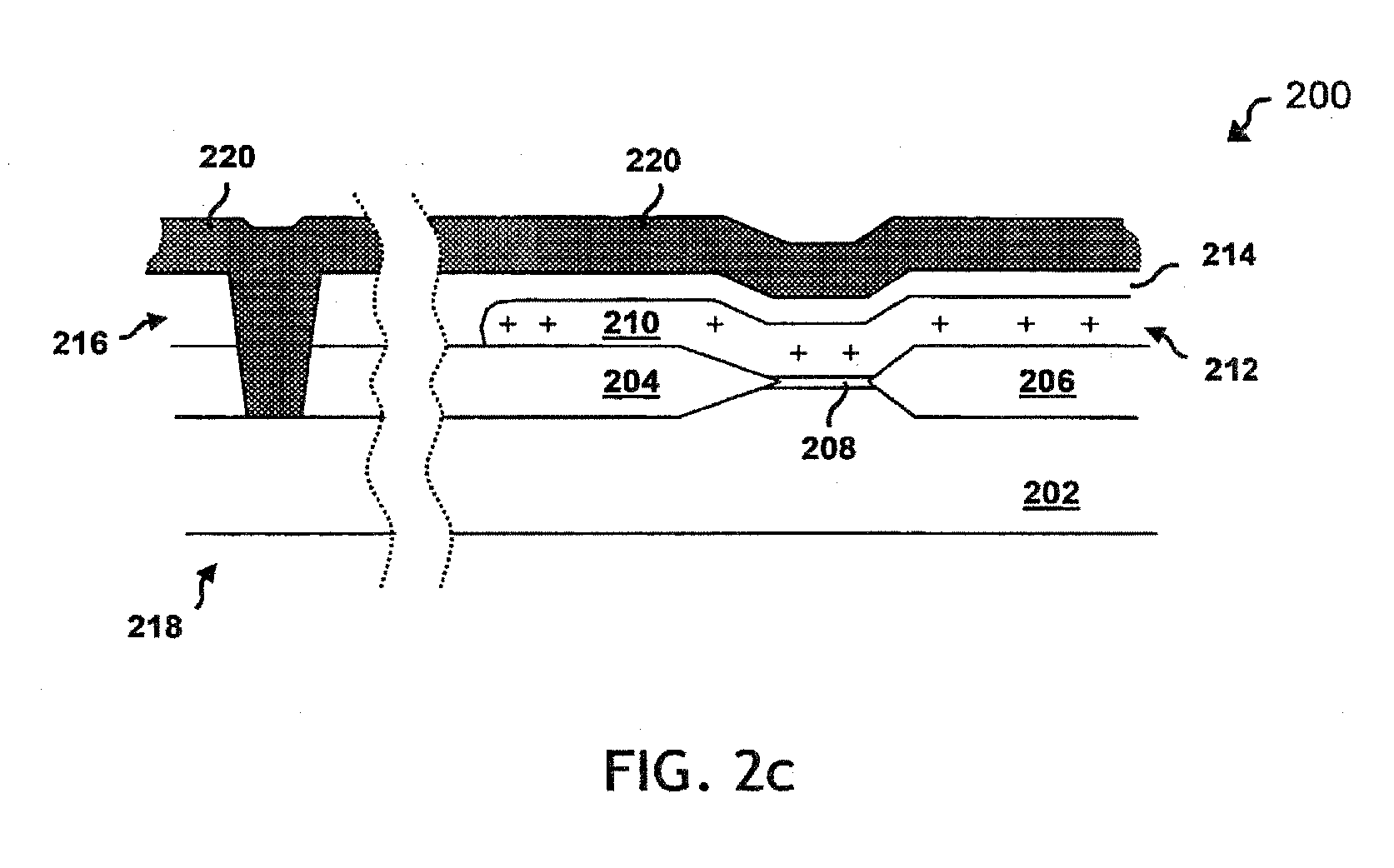
[0019] While the making and using of various embodiments of the present invention are discussed in detail below, it should be appreciated that the present invention provides many applicable inventive concepts, which can be embodied in a wide variety of specific contexts. Certain aspects of the present invention are hereafter illustratively described in conjunction with the formation of semiconductor capacitor structures having polysilicon and metal (e.g., Ti, Al) conductive layers. The specific embodiments discussed herein are, however, merely demonstrative of specific ways to make and use the invention and do not limit the scope of the invention.

[0020] The present invention recognizes that electrical charge is induced in certain conductive semiconductor structures or layers (e.g., polysilicon, metal) during a number of fabrication processes (e.g., deposition, implant, plasma etch). Often that charge accumulates within a particular structure or layer, having no means to dissipate. ...


PUM


Abstract

The present invention provides a system for dissipating any aberrant charge that may accumulate during the fabrication of a semiconductor device segment (200), obviating overstress or break down damage to a focal device structure (208) that might result from uncontrolled dissipation of the aberrant charge. A substrate (202) has first and second intermediate structures (204, 206) disposed atop the substrate, with the focal structure disposed atop the substrate therebetween. A first conductive structure (210) is disposed atop the second intermediate structure, the focal structure, and a portion of the first intermediate structure. A third intermediate structure (214) is disposed contiguously atop the first conductive structure and the first intermediate layer. A void (216) is formed in a peripheral region (218) of device segment, through the first and third intermediate layers down to the substrate. A second conductive structure (220) is disposed atop the third intermediate structure such that it couples the substrate through the void.

Description

TECHNICAL FIELD OF THE INVENTION [0001] The present invention relates generally to the field of semiconductor devices and, more particularly, to apparatus and methods for dissipating transient charge occurring during the formation of certain semiconductor device structures. BACKGROUND OF THE INVENTION [0002] The continual demand for enhanced integrated circuit performance has resulted in, among other things, a dramatic reduction of semiconductor device geometries, and continual efforts to optimize the performance of every substructure within any semiconductor device. A number of improvements and innovations in fabrication processes, material composition, and layout of the active circuit levels of a semiconductor device have resulted in very high-density circuit designs. Increasingly dense circuit design has not only improved a number of performance characteristics, it has also increased the importance of, and attention to, semiconductor material properties and behaviors. [0003] The ...

Claims


Application Information

Patent Timeline
Patent Type & Authority Applications(United States)
IPC IPC(8): H01L29/76
CPCH01L23/62H01L27/0248H01L2924/0002H01L2924/00
Inventor TIAN, WEIDONGSUCHER, BRADLEYIMAM, ZAFAR
Owner TEXAS INSTR INC
Why Eureka
Try Eureka