SOI polysilicon trench refill perimeter oxide anchor scheme

a polysilicon trench and anchor scheme technology, applied in the field of microfabrication techniques, can solve the problems of increasing the overall die area, increasing the parasitic capacitance between the anchor and the substrate, and the size of the anchor perimeter of the device, so as to reduce the die size, minimize the perimeter, and minimize the parasitic capacitance

Inactive Publication Date: 2005-07-05
NORTH STAR INNOVATIONS
View PDF9 Cites 56 Cited by
  • Summary
  • Abstract
  • Description
  • Claims
  • Application Information

AI Technical Summary

Benefits of technology

[0007]In one aspect, a method for creating a MEMS structure is provided herein. In accordance with the method, a substrate is provided having a sacrificial layer disposed thereon and having a layer of silicon disposed over the sacrificial layer. A first trench is created which extends through the silicon layer and the sacrificial layer and which separates the sacrificial layer into a first region enclosed by the first trench and a second region exterior to the first trench. A first material is deposited into the first trench such that the first material fills the first trench to a depth at least equal to the thickness of the sacrificial layer. A second trench is created exterior to the first trench which extend

Problems solved by technology

The methodology depicted in FIGS. 1-3 suffers from a number of drawbacks, one being its reliance on partial chemical etching to define the anchor structure perimeter.
In a fabrication scheme which relies on partial chemical etching, these variations in etch rates result

Method used


Image

  • SOI polysilicon trench refill perimeter oxide anchor scheme
  • SOI polysilicon trench refill perimeter oxide anchor scheme
  • SOI polysilicon trench refill perimeter oxide anchor scheme

Examples


Embodiment Construction

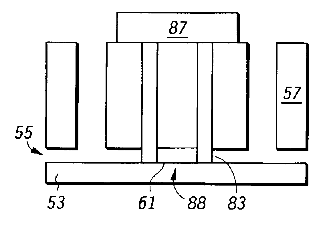
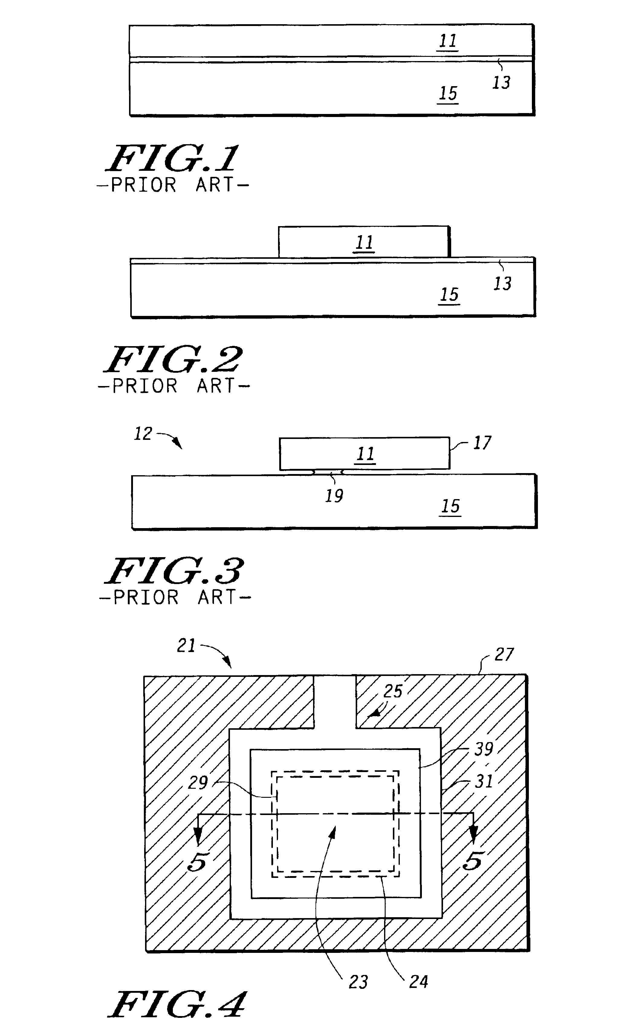
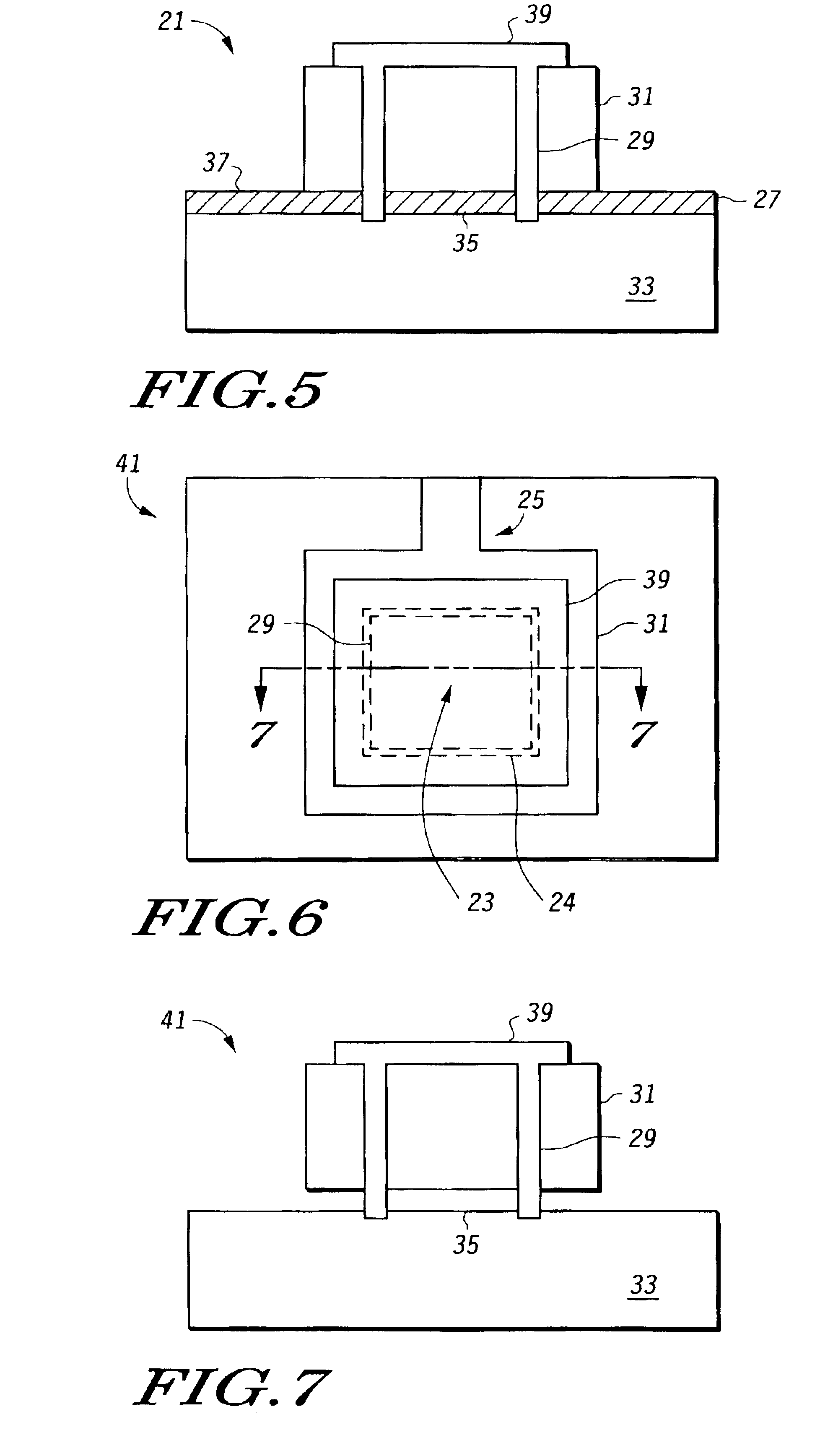
[0021]It has now been discovered that the above noted needs may be met by forming the anchor portion of a MEMS structure in such a way that it is protected during release by a material which is resistant to the etch used to achieve release of the structure. In the case of an SOI device, for example, this may be accomplished by forming a perimeter trench which defines the perimeter of the anchor portion of the device and which extends completely through the silicon and dielectric layers to the surface of the substrate. The trench is then filled with a material which is resistant to the etch used to achieve release of the structure, after which the structure is released by etching away a portion of the dielectric layer external to the perimeter trench. Since the fill material in the trench is resistant to the etch, the perimeter of the anchor portion is not significantly affected by the etch (that is, the dimensions of the anchor perimeter are not dependent on factors such as variatio...


PUM

PropertyMeasurementUnit
Thicknessaaaaaaaaaa

Abstract

A method for creating a MEMS structure is provided. In accordance with the method, a substrate (53) is provided having a sacrificial layer (55) disposed thereon and having a layer of silicon (57) disposed over the sacrificial layer. A first trench (59) is created which extends through the silica layer and the sacrificial layer and which separates the sacrificial layer into a first region (61) enclosed by the first trench and a second region (63) exterior to the first trench. A first material (65) is deposited into the first trench such that the first material fills the first trench to a depth at least equal to the thickness of the sacrificial layer. A second trench (71) is created exterior to the first trench which extends through at least the silicon layer and exposes at least a portion of the second region of the sacrificial layer. The second region of the sacrificial layer is contacted, by way of the second trench, with a chemical etching solution adapted to etch the sacrificial layer, said etching solution being selective to the first material.

Description

FIELD OF THE INVENTION[0001]The present invention relates generally to microfabrication techniques, and more particularly to methods for making an anchor for a MEMS device.BACKGROUND OF THE INVENTION[0002]Advancements in micromachining and other microfabrication techniques and processes have enabled the fabrication of a wide variety of MicroElectroMechanical Systems (MEMS) and devices. These include moving rotors, gears, switches, accelerometers, miniaturized sensors, actuator systems, and other such structures.[0003]One popular approach for forming MEMS devices makes use of a modified wafer known as a Silicon-On-Insulator (SOI) wafer. An SOI wafer is essentially a silicon wafer having a silicon dioxide dielectric layer disposed thereon, and having a thin film of active single-crystalline silicon disposed on the dielectric layer.[0004]FIGS. 1-3 illustrate a conventional method for creating a MEMS structure on an SOI wafer. As shown in FIG. 1, in accordance with this method, a silico...

Claims


Application Information

Patent Timeline
IPC IPC(8): B81B3/00B81C1/00
CPCB81C1/00039B81B2203/0307B81B2203/033B81B2203/0118
Inventor O'BRIEN, GARY J.MONK, DAVID J.
Owner NORTH STAR INNOVATIONS
Why Eureka
Try Eureka