LED device, flip-chip LED package and light reflecting structure

a technology of led devices and flip-chips, applied in the direction of semiconductor devices, basic electric elements, electrical appliances, etc., can solve problems such as the achievement of construction interference of lights, and achieve the effect of enhancing light extraction efficiency

Active Publication Date: 2005-07-05
EPISTAR CORP
View PDF4 Cites 132 Cited by
  • Summary
  • Abstract
  • Description
  • Claims
  • Application Information

AI Technical Summary

Benefits of technology

[0009]Accordingly, the present invention is to provide a light reflective structure, which is applicable for a LED device to enhance the extraction efficiency of light.
[0010]Another object of the present invention is to provide a LED device having a light reflective structure of the present invention, wherein the extraction efficiency of light is enhanced.
[0011]It is yet another object of the present invention to provide a flip-chip LED package structure having a light reflective structure of the present invention, wherein the extraction efficiency of light is enhanced.
[0012]In order to achieve the above objects and other advantages of the present invention, a light reflective structure for a LED device is provided. The light reflective structure includes, for example but not limited to, a transparent conductive oxide layer deposited on a semiconductor layer, a transparent insulating layer deposited on the transparent conductive oxide layer, and a reflecting layer deposited on the transparent insulating layer. The transparent conductive oxide layer is provided as an ohmic contact layer for the semiconductor layer. The transparent insulating layer is provided as a passivation layer for the transparent conductive oxide layer. When the wavelength of the light emitted from the LED device is λ, and the refractive index of the transparent conductive oxide layer is n, the thickness of the transparent conductive oxide layer is preferably to be (2 m+1)λ / 2 n (m is 0 or an positive integer). When the refractive index of the transparent insulating layer is k, the thickness of the transparent insulating layer is preferably to be (2 m+1)λ / 2 k (m is 0 or an positive integer). Therefore, a constructive interference of the lights is achieved.
[0018]Accordingly, in the present invention, the material of the ohmic contact layer includes a transparent conductive metal oxide, and a thermal process for achieving a good ohmic contact is not required for the transparent conductive metal oxide. Therefore, the interface between the ohmic contact layer and the second doped layer is smooth, and thus the interface can be provided as a reflecting surface. Moreover, in the present invention, the absorption to visible light of the transparent conductive metal oxide can be reduced to less than 10% (for example, when the oxide is an indium tin oxide (ITO; therefore, the absorption of the ohmic contact layer to the LED device is reduced drastically.

Problems solved by technology

Therefore, a constructive interference of the lights is achieved.

Method used


Image

  • LED device, flip-chip LED package and light reflecting structure
  • LED device, flip-chip LED package and light reflecting structure
  • LED device, flip-chip LED package and light reflecting structure

Examples


Embodiment Construction

[0024]The present invention now will be described more fully hereinafter with reference to the accompanying drawings, in which preferred embodiments of the invention are shown. This invention may, however, be embodied in many different forms and should not be construed as limited to the embodiments set forth herein; rather, these embodiments are provided so that this disclosure will be thorough and complete, and will fully convey the scope of the invention to those skilled in the art. Like numbers refer to like elements throughout.

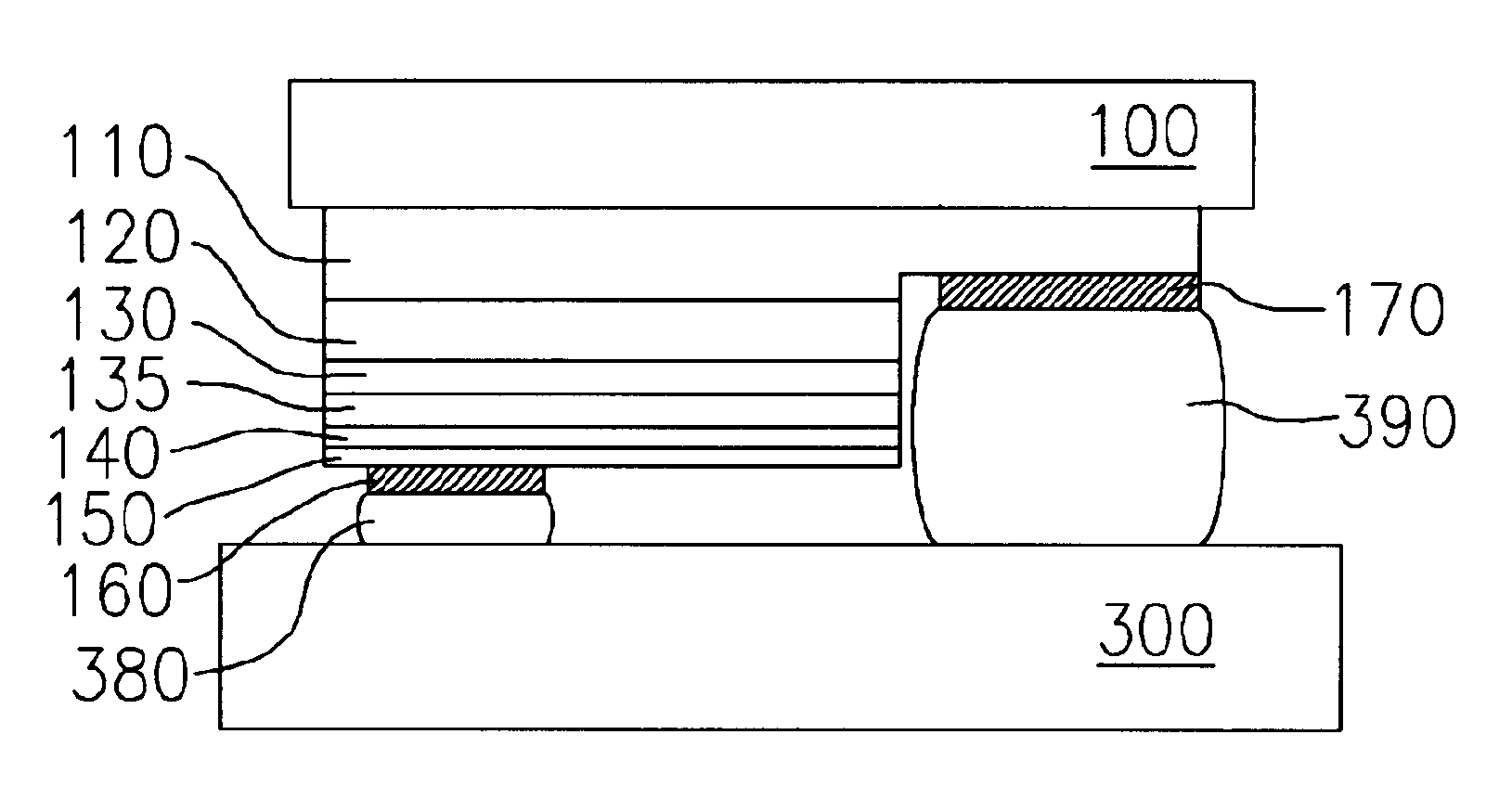
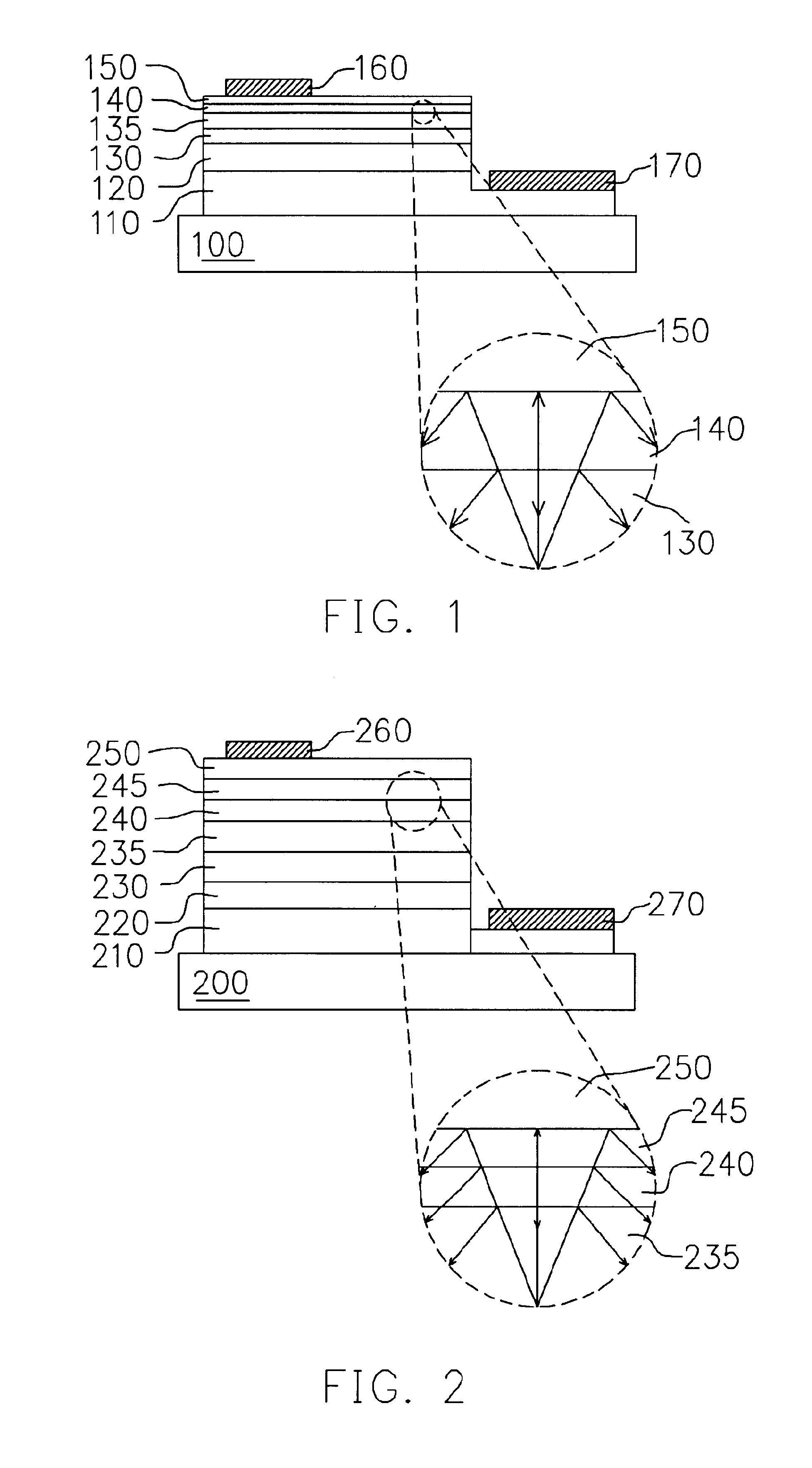
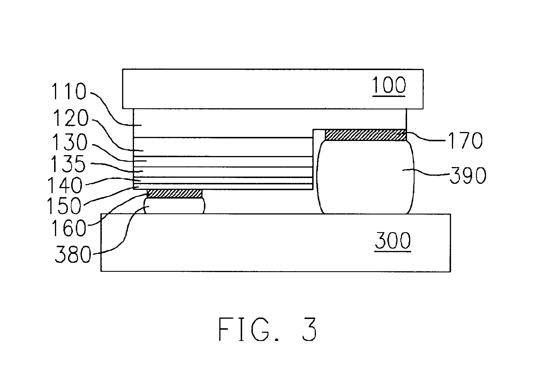
[0025]FIG. 1 is a cross-sectional view illustrating a structure of a LED device and a enlarged view of a portion adjacent to a interface of the transparent conductive oxide layer of the LED device according to a preferred embodiment of the present invention. Referring to FIG. 1, the LED device includes a device substrate 100, a N-type doped layer 110, a light emitting layer 120, a P-type doped layer 130, a strained-layer superlattice (SLS) contact layer 13...


PUM


Abstract

A light emitting diode (LED) device is provided. The LED device includes a device substrate, a first doped layer of a first conductivity type, a light emitting layer, a second doped layer of a second conductivity type, a transparent conductive oxide layer, a reflecting layer and two electrodes. The first doped layer is deposited on the device substrate, the light emitting layer is deposited on a portion of the first doped layer, and the second doped layer is deposited on the light emitting layer. The first and the second doped layers are comprised of III-V semiconductor material respectively. The transparent conductive oxide layer is deposited on the second doped layer, and the reflecting layer is deposited on the transparent conductive oxide layer. The two electrodes are deposited on the reflecting layer and the first doped layer respectively.

Description

CROSS REFERENCE TO RELATED APPLICATIONS[0001]This application claims the priority benefit of Taiwan application serial no.92120195, filed on Jul. 24, 2003.BACKGROUND OF INVENTION[0002]1. Field of the Invention[0003]The invention relates in general to a structure of a semiconductor light emitting device, and more particularly, to a structure of a light emitting diode (LED) device, to a package structure of a flip-chip LED device, and to a light reflective structure being applicable for a LED.[0004]2. Related Art of the Invention[0005]In general, a light emitting diode (LED) constructed by an III-V semiconductor material can be provided as a wide bandgap light emitting device. The wavelength of the light emitted from the wide bandgap light emitting device ranges from infrared (IR) to ultraviolet (UV); therefore the entire spectrum of visible light is also covered. In recent years, due to the rapid development of the high illumination of the gallium nitride (GaN) LEDs having a blue / gre...

Claims


Application Information

Patent Timeline
Patent Type & Authority Patents(United States)
IPC IPC(8): H01L21/00H01L33/00H01L33/04H01L33/40H01L33/42H01L33/46
CPCH01L33/46H01L33/04H01L33/405H01L33/42
Inventor SHEI, SHIH-CHANGSHEU, JINN-KONG
Owner EPISTAR CORP
Why Eureka
Try Eureka