Vertical PNP bipolar transistor

a technology of bipolar transistor and vertical pnp, which is applied in the direction of transistors, semiconductor devices, electrical equipment, etc., can solve the problems of increased manufacturing cost, increased process steps, and inability to avoid the increase in the area of vertical pnp-bipolar transistors, so as to achieve the effect of lowering manufacturing costs

Inactive Publication Date: 2005-07-05
RENESAS ELECTRONICS CORP
View PDF3 Cites 6 Cited by
  • Summary
  • Abstract
  • Description
  • Claims
  • Application Information

AI Technical Summary

Benefits of technology

[0024]Therefore, the object of the present invention is to solve the above-described problems, and to provide a semiconductor device comprising a vertical pnp-bipolar transistor that can isolate the collector layer from the substrate potential without requiring complicated process steps, lower the manufacturing costs, and achieve downsizing, and to provide a method of manufacturing such a semiconductor device.
[0027]According to the present invention, in a semiconductor device comprising a vertical pnp-bipolar transistor in a prescribed element region, by forming a p-type collector layer so as to adhere onto an n-type buried layer of a high concentration, the n-type buried layer can isolate the collector layer from the substrate potential. Also, by forming the p-type collector layer on the n-type buried layer, the p-type collector layer can be formed without special mask alignment, and the further downsizing of the device can be achieved.

Problems solved by technology

Therefore, problems of the complicated process steps, and increase in manufacturing costs arise.
Therefore, increase in the area of the vertical pnp-bipolar transistor cannot be avoided.
This makes the process steps complicated, and results in increase in manufacturing costs.

Method used


Image

  • Vertical PNP bipolar transistor
  • Vertical PNP bipolar transistor
  • Vertical PNP bipolar transistor

Examples


Embodiment Construction

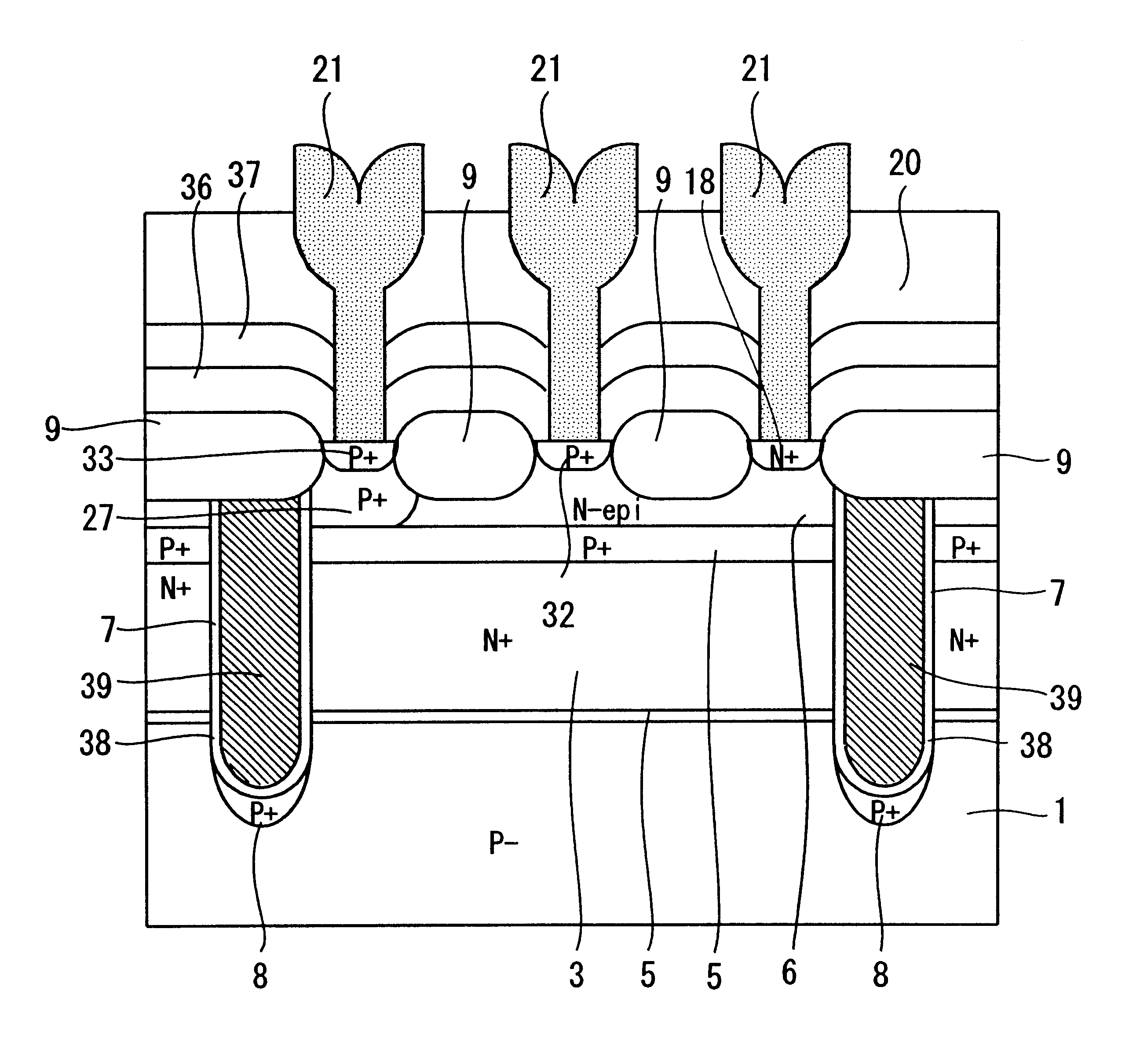
[0037]The embodiments of the present invention will be described below referring to the drawings. FIG. 1 is a schematic sectional view showing the configuration of a semiconductor device according to the embodiment of the present invention. In the semiconductor device according to the embodiment, an epitaxial layer 6 is formed on a buried n+-layer 3 on a p-type silicon semiconductor substrate 1, and a vertical pnp-bipolar transistor (V-PNP) is formed on the epitaxial layer 6 undergone element isolation into islands by a trench isolation structure consisting of trenches formed to left and right of the epitaxial layer 6, and the buried n+-layer 3.

[0038]A buried p+-layer 5 is formed on the n+-layer 3, and the epitaxial layer 6 is formed on the p+-layer 5 on the n+-layer 3. The p+-layer 5 acts as a collector layer of the V-PNP. A p-well 27 is formed as a collector-drawing portion on a part of the buried p+-layer 5, and a collector-leader layer 33 is formed on the surface region of the p...


PUM


Abstract

A semiconductor device in which a vertical pnp-bipolar transistor is formed in a prescribed element region on a semiconductor substrate includes: a buried n+-layer of a high concentration formed in the prescribed element region; and a p-type collector layer formed on the buried n+-layer. By introducing impurities that has a larger diffusion coefficient than the buried n+-layer, the collector layer can be formed on the buried n+-layer formed in common with other element regions, without any special masking.

Description

BACKGROUND OF THE INVENTION[0001]1. Field of the Invention[0002]The present invention relates to a semiconductor device, and a method of manufacturing the same, and more specifically to a semiconductor device comprising a vertical pnp (V-PNP) bipolar transistor, and a method of manufacturing such a semiconductor device.[0003]2. Background Art[0004]Recent semiconductor integrated circuits, for example, bipolar integrated circuits have a structure wherein both npn-bipolar transistors and vertical pnp-bipolar transistors are packaged together. Also as represented by a BiCMOS, various elements, such as npn-bipolar transistors, MOS transistors, and pnp-bipolar transistors may be packaged together on the same substrate to constitute one chip.[0005]FIGS. 6 to 8 are schematic sectional views for illustrating the sequence of process steps of a method of manufacturing a conventional bipolar integrated circuit wherein an npn-bipolar transistor (NPN), an lateral pnp-bipolar transistor (L-PNP), ...

Claims


Application Information

Patent Timeline
Patent Type & Authority Patents(United States)
IPC IPC(8): H01L21/331H01L29/732H01L21/70H01L21/02H01L21/8249H01L29/66H01L27/06H01L21/76H01L21/761H01L21/8222H01L21/8228H01L21/8248H01L27/082
CPCH01L21/8249H01L27/0623H01L29/66272H01L29/732
Inventor FUJII, HIDENORI
Owner RENESAS ELECTRONICS CORP
Why Eureka
Try Eureka