High voltage supply sensing high input resistance operational amplifier input stage

a high-input resistance, operational amplifier technology, applied in differential amplifiers, amplifiers with only semiconductor devices, amplifier details, etc., can solve the problems of poor 1/f noise performance, high-voltage pmos or jfet devices are not available,

Inactive Publication Date: 2005-07-05
NAT SEMICON CORP
View PDF2 Cites 21 Cited by
  • Summary
  • Abstract
  • Description
  • Claims
  • Application Information

AI Technical Summary

Problems solved by technology

In many semiconductor BiCMOS processes, such high voltage PMOS or JFET devices are not available or they suffer from parametric issues such as poor 1 / f noise performance due to compromises made during fabrication.

Method used


Image

  • High voltage supply sensing high input resistance operational amplifier input stage
  • High voltage supply sensing high input resistance operational amplifier input stage
  • High voltage supply sensing high input resistance operational amplifier input stage

Examples


Embodiment Construction

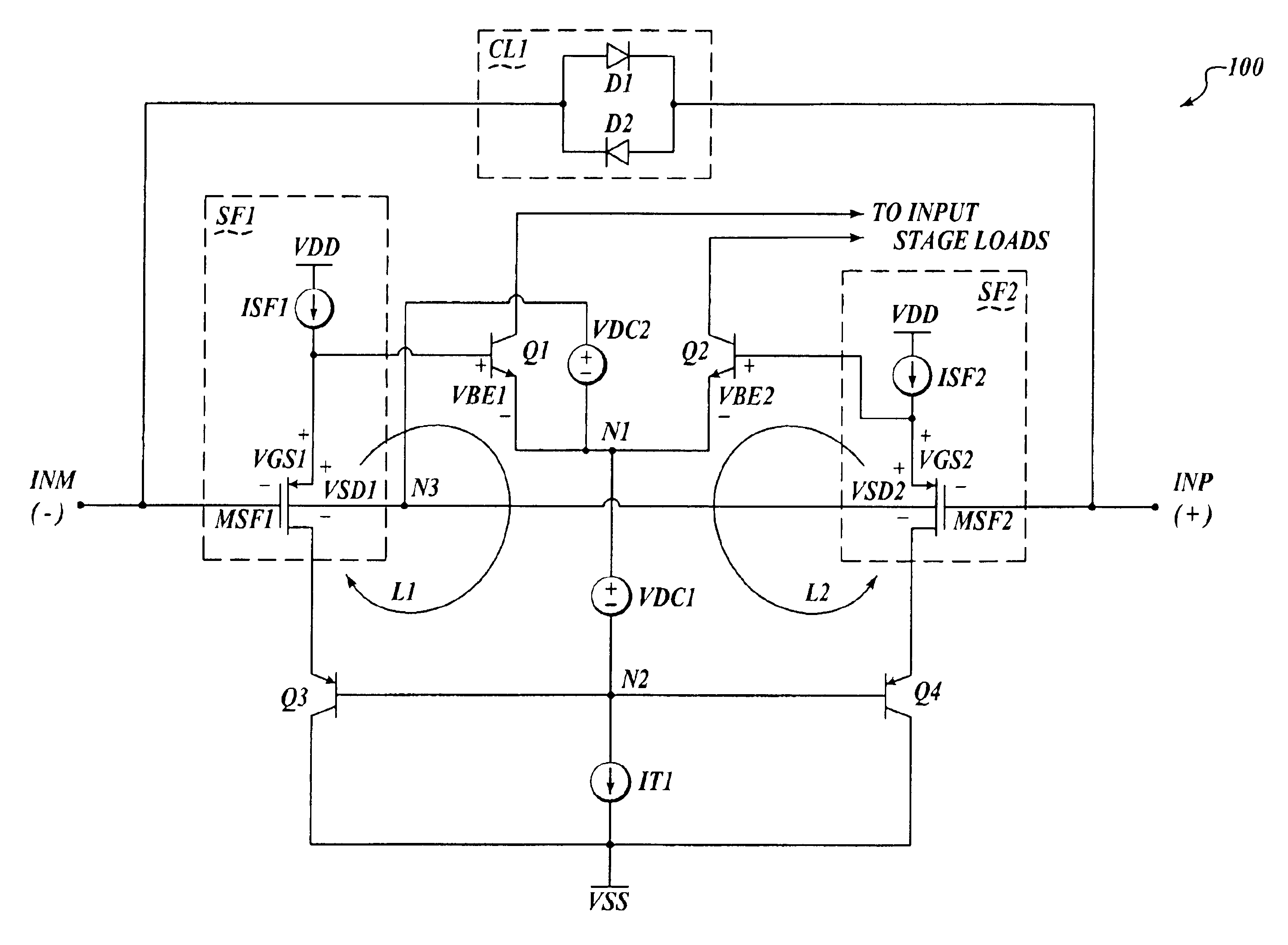
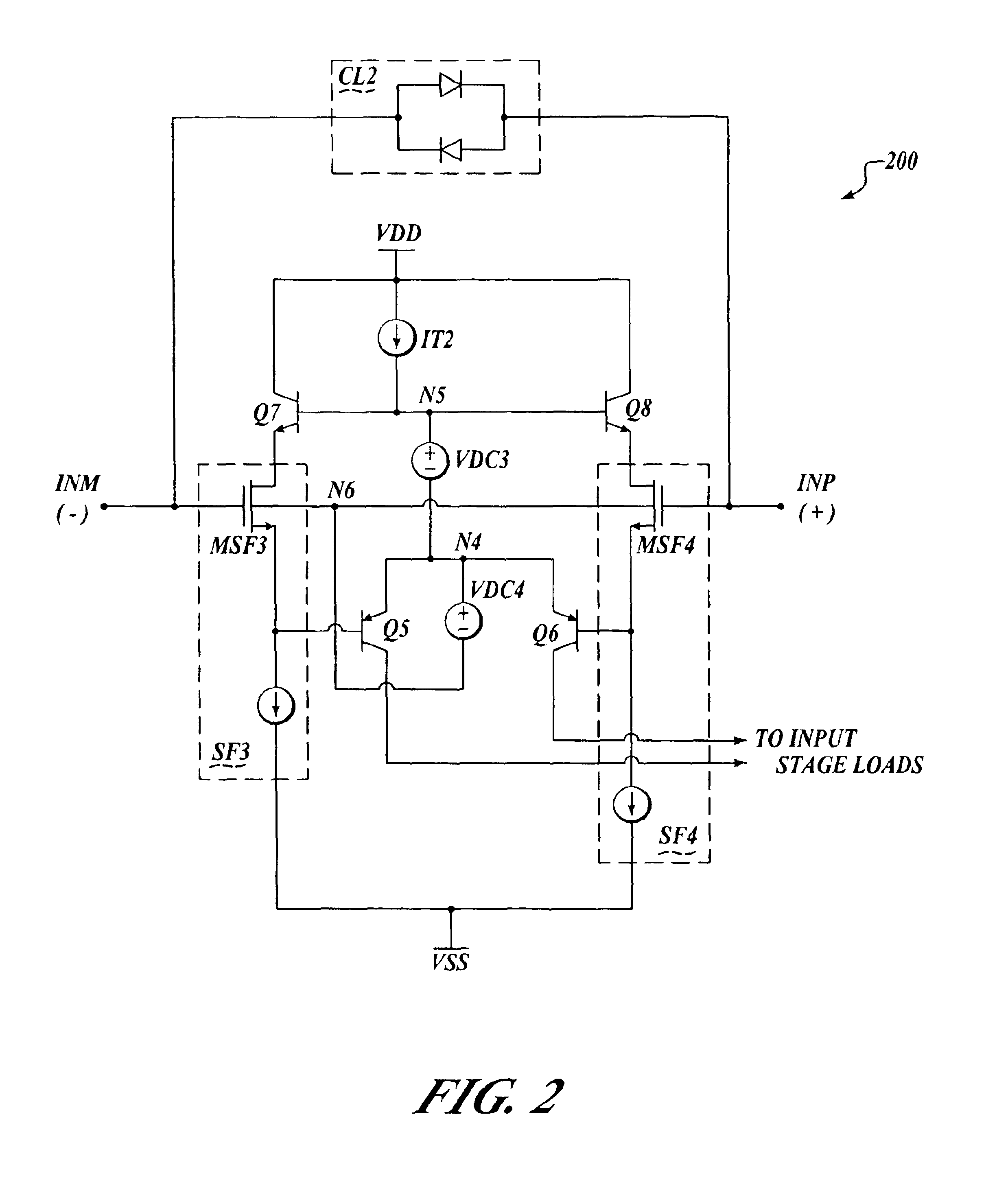
[0007]Various embodiments of the present invention will be described in detail with reference to the drawings, where like reference numerals represent like parts and assemblies throughout the several views. Reference to various embodiments does not limit the scope of the invention, which is limited only by the scope of the claims attached hereto. Additionally, any examples set forth in this specification are not intended to be limiting and merely set forth some of the many possible embodiments for the claimed invention.

[0008]Throughout the specification and claims, the following terms take at least the meanings explicitly associated herein, unless the context clearly dictates otherwise. The meaning of “a,”“an,” and “the” includes plural reference. The meaning of “in” includes “in” and “on.” The term “connected” means a direct connection between the items connected, without any intermediate devices. The term “coupled” refers to both direct connections between the items connected, and...


PUM


Abstract

A high voltage operational amplifier input stage utilizes a pair of low voltage p-type MOSFET input devices configured to operate at a common mode voltage. The input stage operates between positive and negative voltage supply rails. Common mode bipolar transistor feedback loops force drains of the MOSFETs to track corresponding source potentials. MOSFET substrate connections are maintained at a predetermined level above (or below, depending on the power supply sensing arrangement) the common mode voltage of the input stage to ensure power supply sensing capability. The input stage has a common mode range which includes the supply rail potential, and which tolerates a total supply voltage that exceeds the MOSFET breakdown voltage. The effective threshold voltage of the input devices is increased above the nominal threshold value to sustain the linear operation of the input stage.

Description

FIELD OF THE INVENTION[0001]The present invention relates to an input stage of an operational amplifier. More particularly, the present invention relates to a high voltage supply sensing high input resistance operational amplifier input stage that utilizes low voltage MOSFET input devices.BACKGROUND OF THE INVENTION[0002]Implementation of a high voltage operational amplifier having a high input impedance and a common mode input range which includes a negative supply can be achieved using high voltage PMOS or JFET input devices in a traditional differential input stage. In many semiconductor BiCMOS processes, such high voltage PMOS or JFET devices are not available or they suffer from parametric issues such as poor 1 / f noise performance due to compromises made during fabrication.BRIEF DESCRIPTION OF THE DRAWINGS[0003]FIG. 1 is a schematic diagram of an example operational amplifier input stage;[0004]FIG. 2 is a schematic diagram of an example operational amplifier input stage;[0005]F...

Claims


Application Information

Patent Timeline
Patent Type & Authority Patents(United States)
IPC IPC(8): H03F3/45H03F1/32
CPCH03F1/3211H03F3/4508H03F3/45179H03F2203/45511
Inventor CARROLL, KENNETH J.
Owner NAT SEMICON CORP
Why Eureka
Try Eureka