Dual loop sensing scheme for resistive memory elements

a sensing scheme and memory element technology, applied in the direction of information storage, static storage, digital storage, etc., can solve the problems of difficult sensing of the logic state of an mram memory element, and the sensing scheme is vulnerable to stochastic noise, so as to improve the sensitivity of the sensing circuit

Inactive Publication Date: 2005-07-05
OVONYX MEMORY TECH LLC
View PDF6 Cites 76 Cited by
  • Summary
  • Abstract
  • Description
  • Claims
  • Application Information

AI Technical Summary

Benefits of technology

[0014]According to one aspect of the present invention, MRAM cell logic state is sensed by configuring an memory cell so as to form a sensing voltage across the cell that is related to a resistance of the cell. The sensing voltage is applied to an input of a transconductance amplifier, which outputs a sensing current related to the sensing voltage. The sensing current is integrated over time with an additional current and filtered through a digital counter to improve sensing circuit sensitivity.

Problems solved by technology

Nonetheless sensing the logic state of an MRAM memory element is difficult because the technology of the MRAM device imposes multiple constraints.
As shown in FIG. 3, however, this sensing scheme is vulnerable to stochastic noise.
The resulting measurement produces an erroneous result when the noisy voltage signal crosses the reference voltage (Vref) threshold at time terr.

Method used


Image

  • Dual loop sensing scheme for resistive memory elements
  • Dual loop sensing scheme for resistive memory elements
  • Dual loop sensing scheme for resistive memory elements

Examples


Embodiment Construction

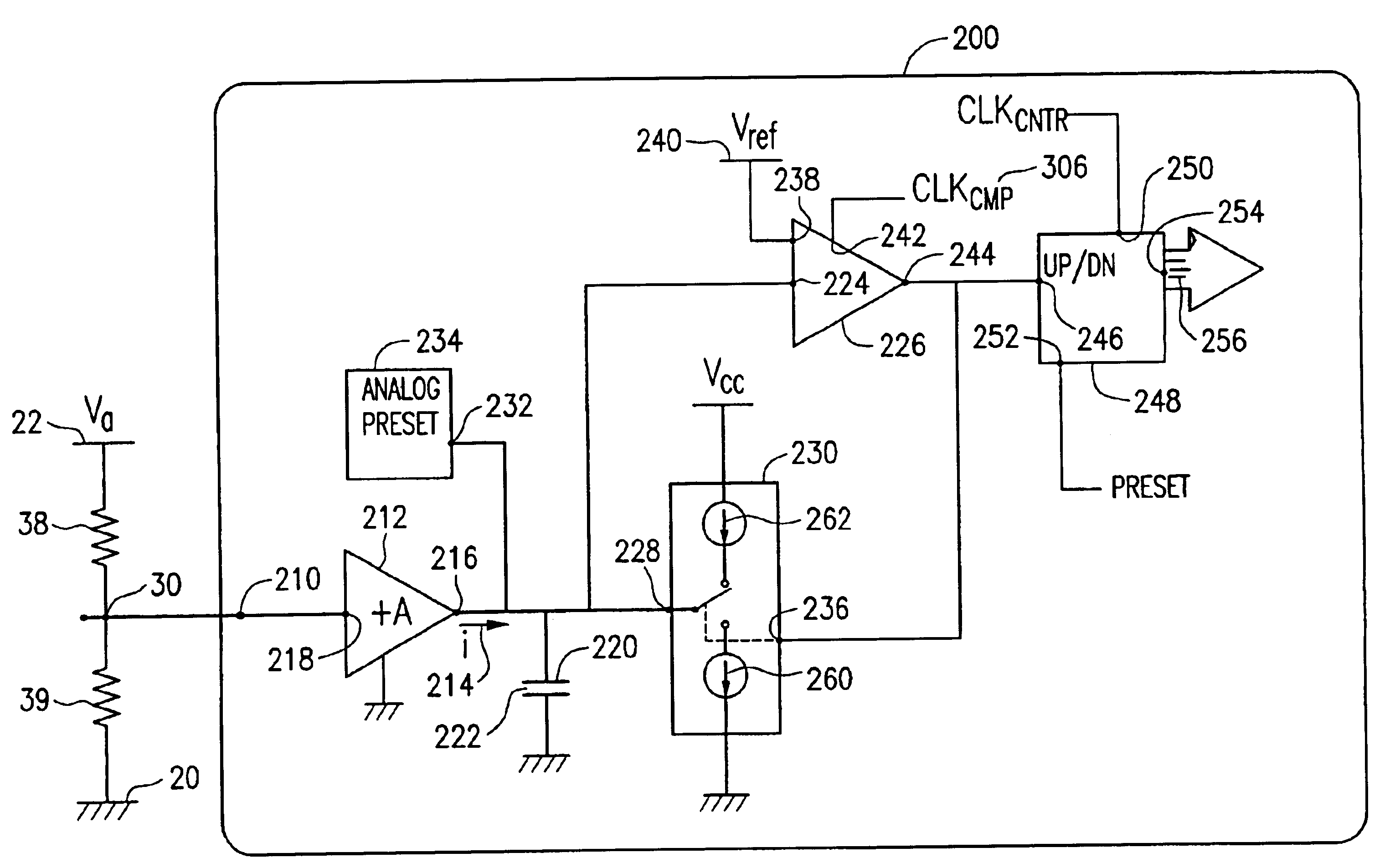
[0030]The present invention operates by receiving a signal, representing a programmed resistance state of a resistive memory cell, at a digital counter. A resulting digital count value, taken after a sensing time interval, represents the resistance state of the memory cell. Because the count value is digitized and acquired over an extended time, high-frequency stochastic noise in the system is filtered out.

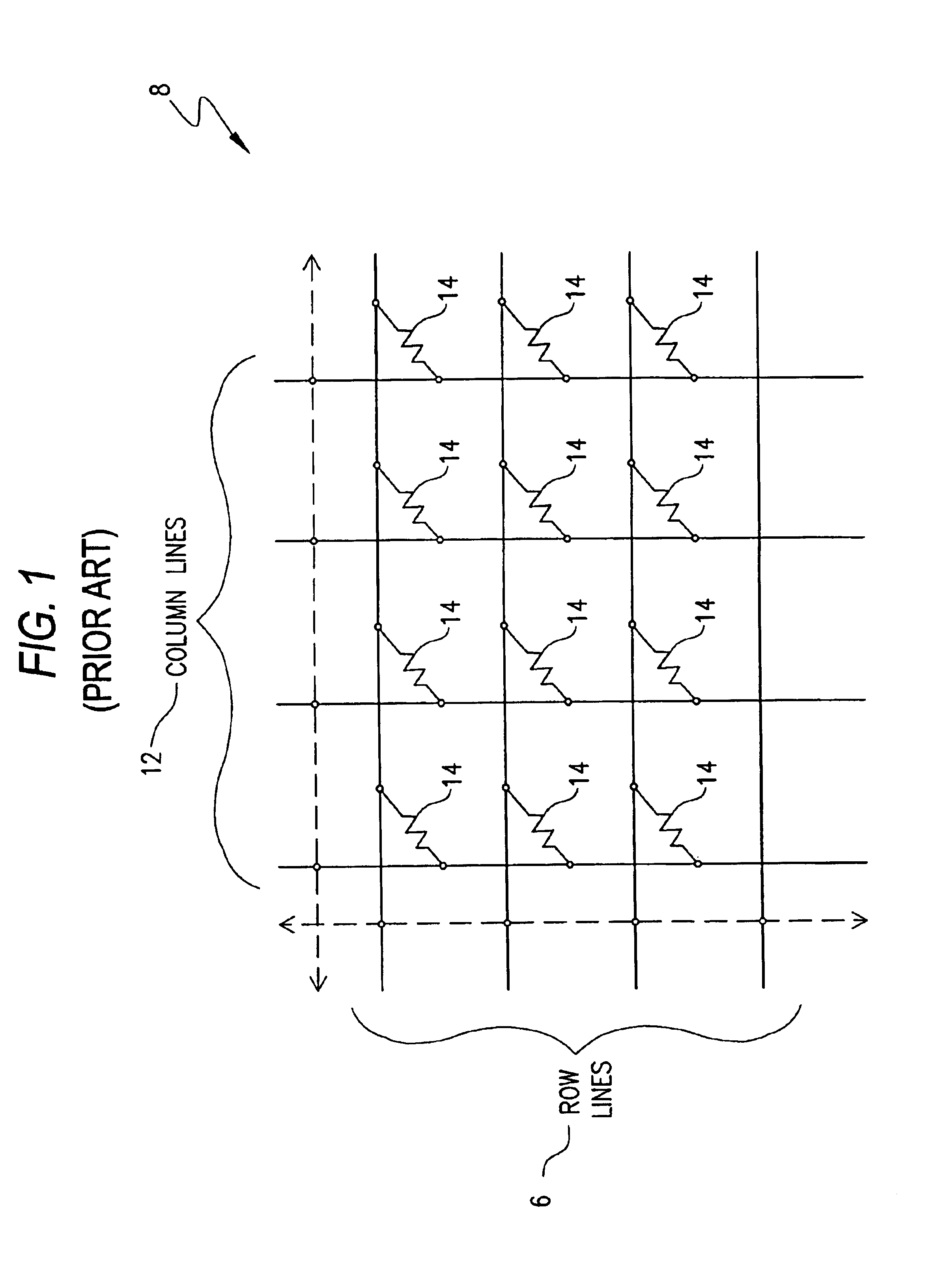
[0031]FIG. 4 shows, in schematic overview, a portion of a memory device according to one aspect of the invention. A crosspoint array of resistive memory cells are configured so that resistance of a particular memory cell may be represented by a sensing voltage. The device 5 includes an array 8 of MRAM cells 14, a plurality of spaced electrically conductive row lines 6, and a plurality of spaced electrically conductive column lines 12. The plurality of row lines 6 is disposed substantially orthogonally to the plurality of column lines 12, defining a plurality of overlap regions at ...


PUM


Abstract

A method and apparatus for sensing a resistive state of a resistive memory element includes producing a first current related to a resistance of a memory cell. The first current is added to a second current during a first sensing time and subtracted from a third current during a second sensing time. The first, second and third currents are integrated over time using a capacitor, and a resulting voltage signal on the capacitor is timed using a clocked counter. A time average value of a digital output of the clocked counter is then related to the resistance of the memory cell, and hence to the resistive state of the resistive memory element.

Description

[0001]This application is a divisional of application Ser. No. 10 / 222,843, filed on Aug. 19, 2002 now U.S. Pat. No. 6,892,188 issued on Dec. 7, 2004, which is incorporated herein by reference.BACKGROUND OF THE INVENTION[0002]1. Field of the Invention[0003]The present invention relates to the reading of resistor-based memory devices such as magneto-resistive random access memory (MRAM) devices which store logic values as resistive states in a memory cell.[0004]2. Description of the Related Art[0005]FIG. 1 shows one example of a resistor based memory array architecture called a crosspoint array. The memory array 8 includes a plurality of row lines 6 arranged orthogonally to a plurality of column lines 12. Each row line is coupled to each of the column lines by a respective resistive memory cell 14. The resistance value of each memory cell stores one of two or more logical values depending on which of a plurality of resistance values it is programmed to exhibit. A characteristic of the...

Claims


Application Information

Patent Timeline
Patent Type & Authority Patents(United States)
IPC IPC(8): G11C7/06G11C11/16G11C11/02G11C11/15
CPCG11C7/06G11C11/16G11C13/0061G11C13/004G11C2013/0057G11C11/1673G11C11/1693G11C11/15
Inventor BAKER, R. JACOB
Owner OVONYX MEMORY TECH LLC
Why Eureka
Try Eureka