Optimal buffered routing path constructions for single and multiple clock domains systems

a routing path and clock domain technology, applied in the field of automatic layout of integrated circuits, can solve the problems of slow path algorithm, delay and signal loss of integrated circuit connections, and physical components (i.e., wires) with non-ideal properties,

Active Publication Date: 2005-07-05
IBM CORP
View PDF2 Cites 30 Cited by
  • Summary
  • Abstract
  • Description
  • Claims
  • Application Information

AI Technical Summary

Benefits of technology

[0023]The present invention is directed toward a method, computer program product, and data processing system for automatically designing routing paths in an integrated circuit. The present invention allows fo

Problems solved by technology

The reason for this is that the connections themselves are physical components (i.e., wires) with non-ideal properties.
Like all electrical conductors, integrated circuit connections suffer from delay and signal loss due to physical properties such as resistance, capacitance, and relativistic limitations on the speed at which electrons are able to travel.
The Fast Path algorithm is somewhat limited in its application, however.

Method used


Image

  • Optimal buffered routing path constructions for single and multiple clock domains systems
  • Optimal buffered routing path constructions for single and multiple clock domains systems
  • Optimal buffered routing path constructions for single and multiple clock domains systems

Examples


Embodiment Construction

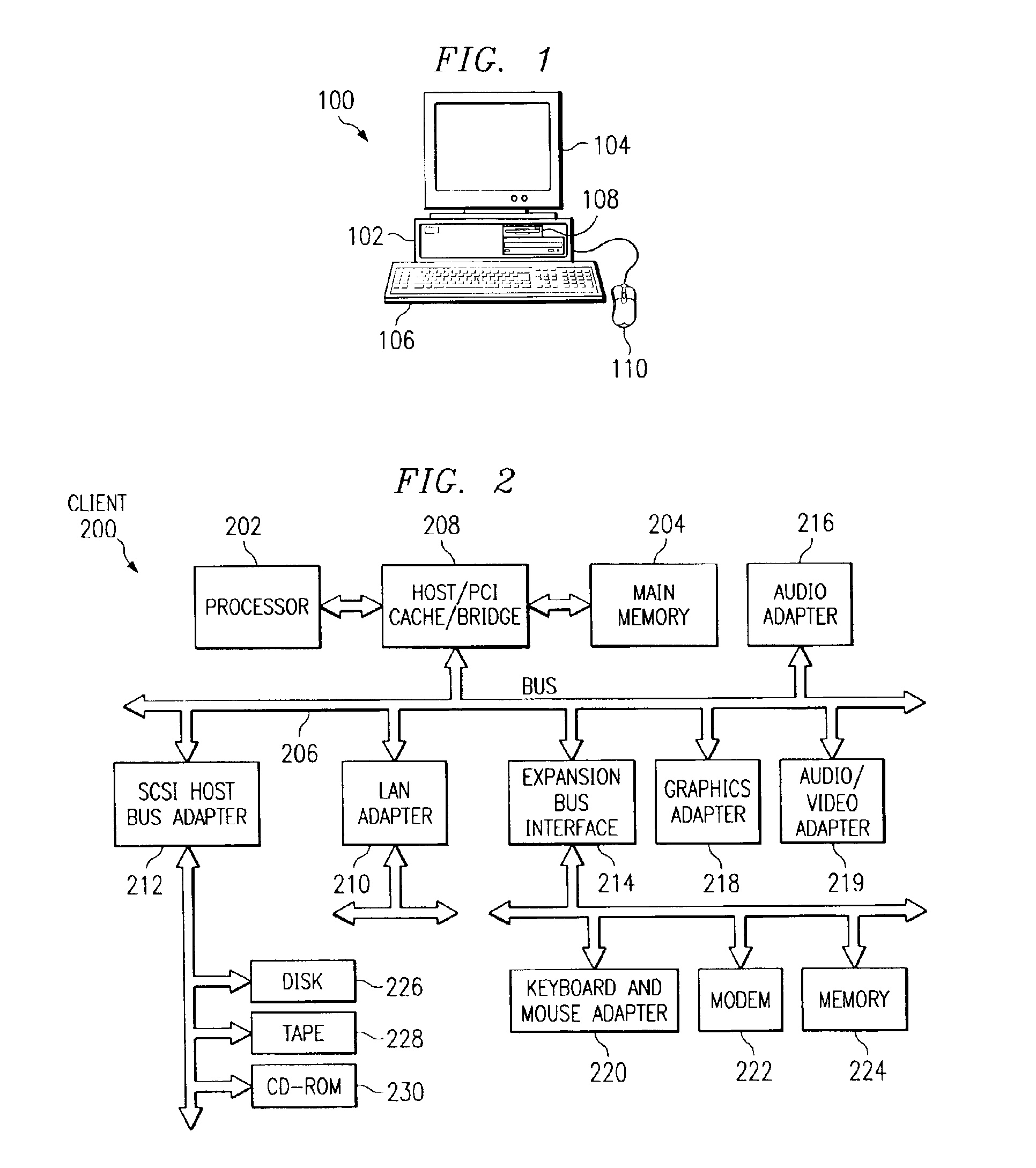
[0038]With reference now to the figures and in particular with reference to FIG. 1, a pictorial representation of a data processing system in which the present invention may be implemented is depicted in accordance with a preferred embodiment of the present invention. A computer 100 is depicted which includes system unit 102, video display terminal 104, keyboard 106, storage devices 108, which may include floppy drives and other types of permanent and removable storage media, and mouse 110. Additional input devices may be included with personal computer 100, such as, for example, a joystick, touchpad, touch screen, trackball, microphone, and the like. Computer 100 can be implemented using any suitable computer, such as an IBM eServer computer or IntelliStation computer, which are products of International Business Machines Corporation, located in Armonk, N.Y. Although the depicted representation shows a computer, other embodiments of the present invention may be implemented in other...


PUM


Abstract

A method, computer program product, and data processing system for automatically designing routing paths in an integrated circuit is disclosed. The present invention allows for the design of paths that are optimal in terms of the signal delay in circuits that may require registers for signal to travel over multiple clock cycles or in circuits that may contain multiple clock domains.
An integrated circuit die is modeled as a weighted grid graph in which the edges represent wire segments and the weights represent the delays associated with those wire segments. Designing for optimum delay involves finding a shortest path between two vertices in the grid graph using a modified single-source shortest path algorithm. Registers, buffers, and dual-clock domain synchronizers are modeled according to a labeling function that assigns components to selected vertices in the routing path for optimal results.

Description

BACKGROUND OF THE INVENTION[0001]1. Technical Field[0002]The present invention relates generally to the automated layout of integrated circuits. In particular, the present invention is directed toward automatic generation of optimized wire routing in very large scale integration (VLSI) circuits.[0003]2. Description of Related Art[0004]In recent years, it has become commonplace for integrated circuit designers to build an integrated circuit layout from libraries of reusable high-level modules, sometimes referred to as “macro blocks.” Proprietary macro blocks are often referred to as “intellectual property blocks” (“IP blocks”), to emphasize their relatively intangible, yet proprietary nature. Computerized integrated circuit design tools may be used to store, retrieve, and combine macro blocks into complete integrated circuits. This design philosophy of combining reusable macro blocks to produce a complex integrated circuit is known as “system-on-a-chip” (SoC) design.[0005]Designing a...

Claims


Application Information

Patent Timeline
IPC IPC(8): G06F12/00G06F3/00G06F17/50
CPCG06F17/5077G06F30/394
Inventor ALPERT, CHARLES JAYHASSOUN, SOHA
Owner IBM CORP
Why Eureka
Try Eureka