EEPROM memory cell and method of forming the same

a memory cell and memory cell technology, applied in the field of eeprom memory cell structure, can solve the problems of inability to continuously increase the electric field of the insulation layer, the thickness of the dielectric layer cannot be continuously decreased, and the difficulty of widely forming the floating gate on the substrate, etc., to achieve the effect of reducing the area of the cell region and high integration of the semiconductor devi

Inactive Publication Date: 2005-07-12
SAMSUNG ELECTRONICS CO LTD
View PDF7 Cites 25 Cited by
  • Summary
  • Abstract
  • Description
  • Claims
  • Application Information

AI Technical Summary

Benefits of technology

[0014]It is therefore a feature of the present invention to provide an EEPROM memory cell and a method of forming the same, which can erase and program data with reliability, and also can reduce each area of a cell region and a floating gate to achieve a high integration of a semiconductor device.
[0015]It is another feature of the present invention to provide an EEPROM memory cell and a method of forming the same, which can reduce a minimum value of an operating voltage in order to erase and program data with reliability.

Problems solved by technology

Accordingly, it is difficult to widely form the floating gate on the substrate.
Therefore, a thickness of the dielectric layer cannot be continuously decreased.
Meanwhile, due to a breakdown voltage limit, an electric field of the insulation layer cannot be continuously increased with an increase in a voltage applied to the control gate.

Method used


Image

  • EEPROM memory cell and method of forming the same
  • EEPROM memory cell and method of forming the same
  • EEPROM memory cell and method of forming the same

Examples


Embodiment Construction

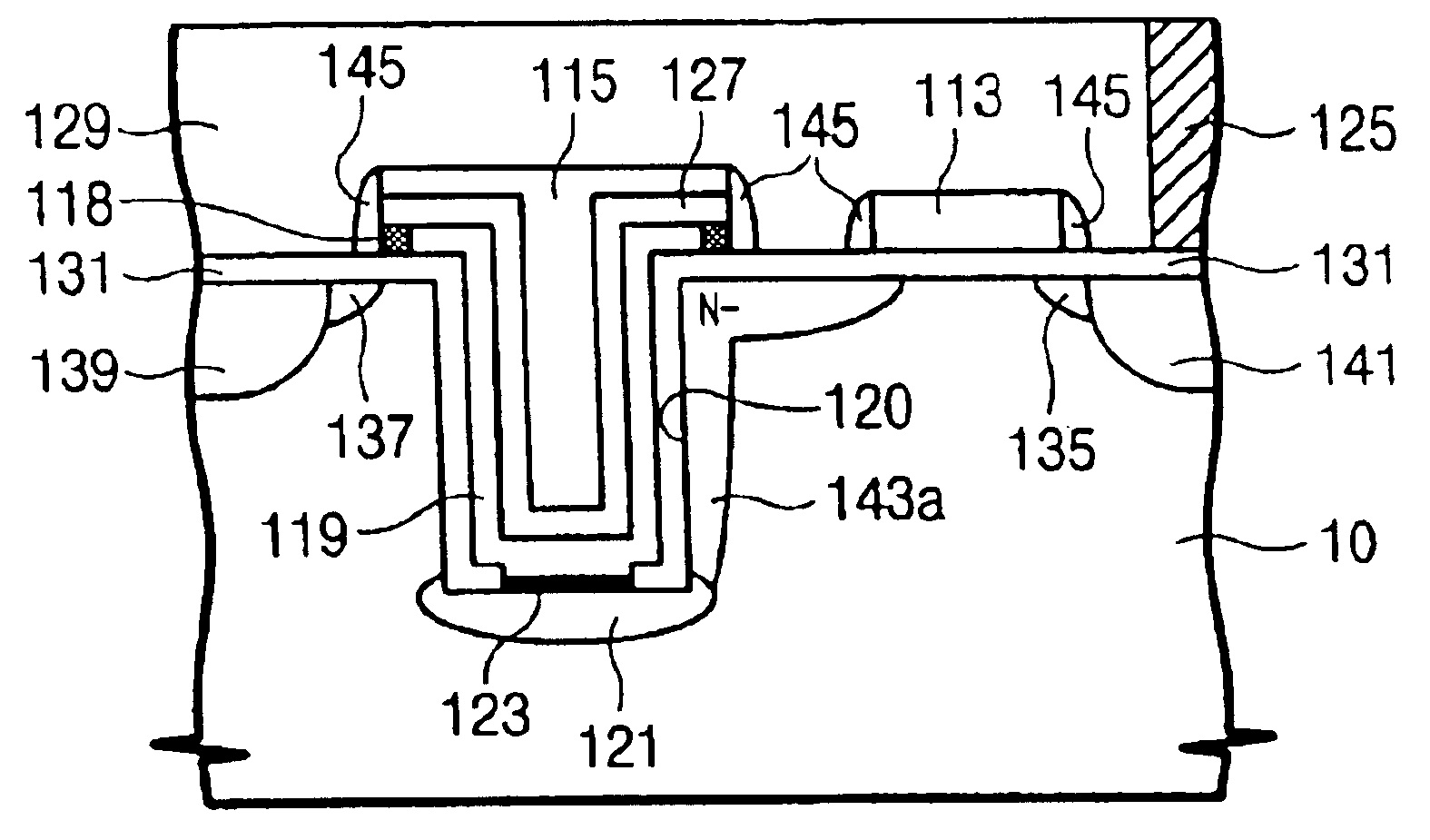
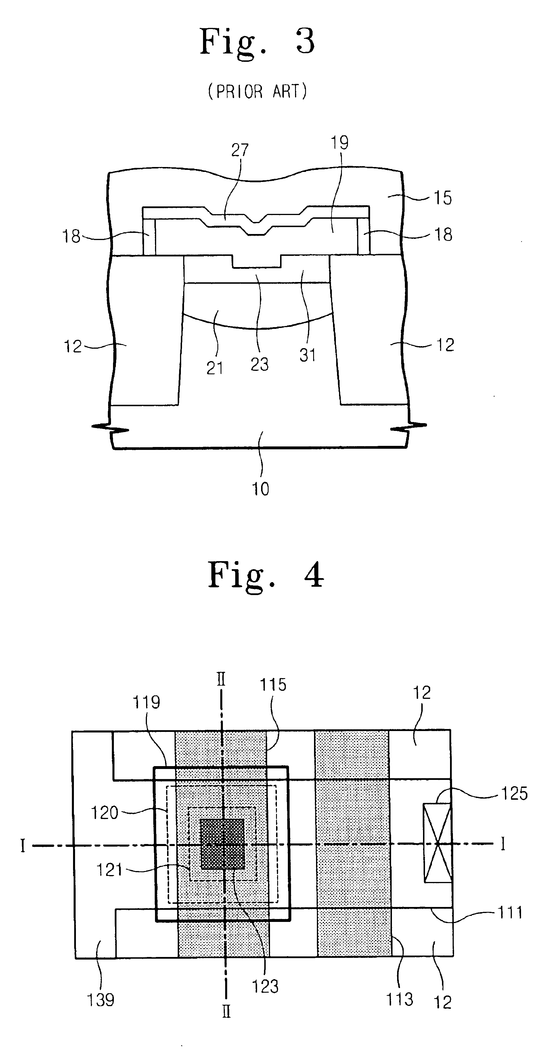
[0025]FIG. 4 is a top plan view showing an EEPROM memory cell in accordance to a first embodiment of the present invention. FIGS. 5 and 6 are cross-sectional views taken along lines I—I and II—II of FIG. 4, respectively.

[0026]Referring to FIG. 4, a device isolation layer is formed to define an active region 111 in one direction. A common source line 139 is formed perpendicularly to the active region 111. A bit line contact 125 is formed at the active region 111. A sensing line 115 and a word line 113 are formed across the active region between the common source line 139 and the bit line contact 125. A trench 120 is formed at the active region 111 under the sensing line 115. Generally, an upper part of the trench 120 is formed wider than a bottom of the trench 20. A floating gate 119 is formed over the trench 120. The floating gate 119 is wider than the upper part of the trench 120 by a certain width to all directions. A tunneling insulation layer 123 is formed in the trench 120. The...


PUM


Abstract

An EEPROM memory cell and a method of forming the same are provided. A portion of a floating gate is formed on walls of a trench formed on the substrate. An inside of the trench is filled with a gate electrode layer constituting a sensing line. This leads to increases in opposite areas of a floating gate and a control gate of a sensing transistor, and a decrease in an area of the floating gate in the substrate. The method of forming an EEPROM memory cell comprises forming a trench in an active area in which a sensing transistor of the substrate will be formed; forming a gate insulation layer including a tunneling insulation layer on an entire surface of the substrate including an inside of the trench; conformally forming a first conductive layer covering the inside of the trench after forming the gate insulation layer; conformally forming a dielectric layer on the first conductive layer; forming a floating gate by patterning the first conductive layer; and stacking and patterning a second conductive layer on the dielectric layer to form a word line and a sensing line.

Description

RELATED APPLICATION[0001]This application is a divisional of U.S. application Ser. No. 10 / 210,446, filed on Aug. 1, 2002 now U.S. Pat. No. 6,744,097, which relies for priority upon Korean Patent Application No. 01-46775, filed on Aug. 2, 2001, the contents of which are herein incorporated by reference in their entirety.FIELD OF THE INVENTION[0002]The present invention relates to an EEPROM memory cell structure and a method of forming the same. More specifically, the invention is directed to an EEPROM memory cell structure and a method of forming the same, which can not only maintain operation characteristics, but also reduce area of an EEPROM cell.BACK OF THE INVENTION[0003]An EEPROM memory is a nonvolatile memory that is semi-permanently capable of retaining data in a memory cell even while power is not applied. In particular, the EEPROM memory is an electrically programmable and erasable memory device.[0004]FIG. 1 is a top plan view showing a typical EEPROM memory cell, and FIGS. ...

Claims


Application Information

Patent Timeline
Patent Type & Authority Patents(United States)
IPC IPC(8): H01L21/28H01L29/423H01L21/02H01L29/40H01L29/66H01L29/788H01L27/115H01L21/8247
CPCH01L21/28273H01L29/42324H01L29/7883H01L29/40114H01L29/788H10B99/00H10B69/00
Inventor YOO, HYUN-KHE
Owner SAMSUNG ELECTRONICS CO LTD
Why Eureka
Try Eureka