
Delay locked loop having low jitter in semiconductor device

a technology of semiconductor devices and locked loops, applied in the field of semiconductor devices, can solve the problems of time delay generation, increased power consumption and area, and sensitive variation of delay according to noise, and achieve the effect of reducing jitter

Inactive Publication Date: 2005-07-12
SK HYNIX INC
View PDF15 Cites 59 Cited by
  • Summary
  • Abstract
  • Description
  • Claims
  • Application Information

AI Technical Summary

Benefits of technology

The present invention provides a delay locked loop (DLL) circuit that reduces jitter by using a digital phase mixer for mixing signals outputted from two delay lines. The circuit includes a delay model unit, an input buffer, a phase detection unit, a control unit, a delay unit, and an output buffer. The technical effect of this invention is to improve the accuracy and reliability of the output clock signal.

Problems solved by technology

At this time, a time delay is generated when the clock signal provided from the external circuit is used in an internal circuit.
In the conventional DLL circuit, since one cycle delay line is required to cover a clock frequency to be used in a system, there is a problem that the delay is sensitively varied according to a noise.
Also, since the DLL circuit is structured with the one cycle delay line, power consumption and area are increased and, after delay is locked, there is a problem that a jitter may be increased due to a noise of a unit delay in the delay line 140.

Method used


Image

  • Delay locked loop having low jitter in semiconductor device
  • Delay locked loop having low jitter in semiconductor device
  • Delay locked loop having low jitter in semiconductor device

Examples


Embodiment Construction

[0010]Hereinafter, a delay locked loop (DLL) circuit having a low jitter by using a digital phase mixer for mixing signals outputted from two delay lines an according to the present invention will be described in detail referring to the accompanying drawings.

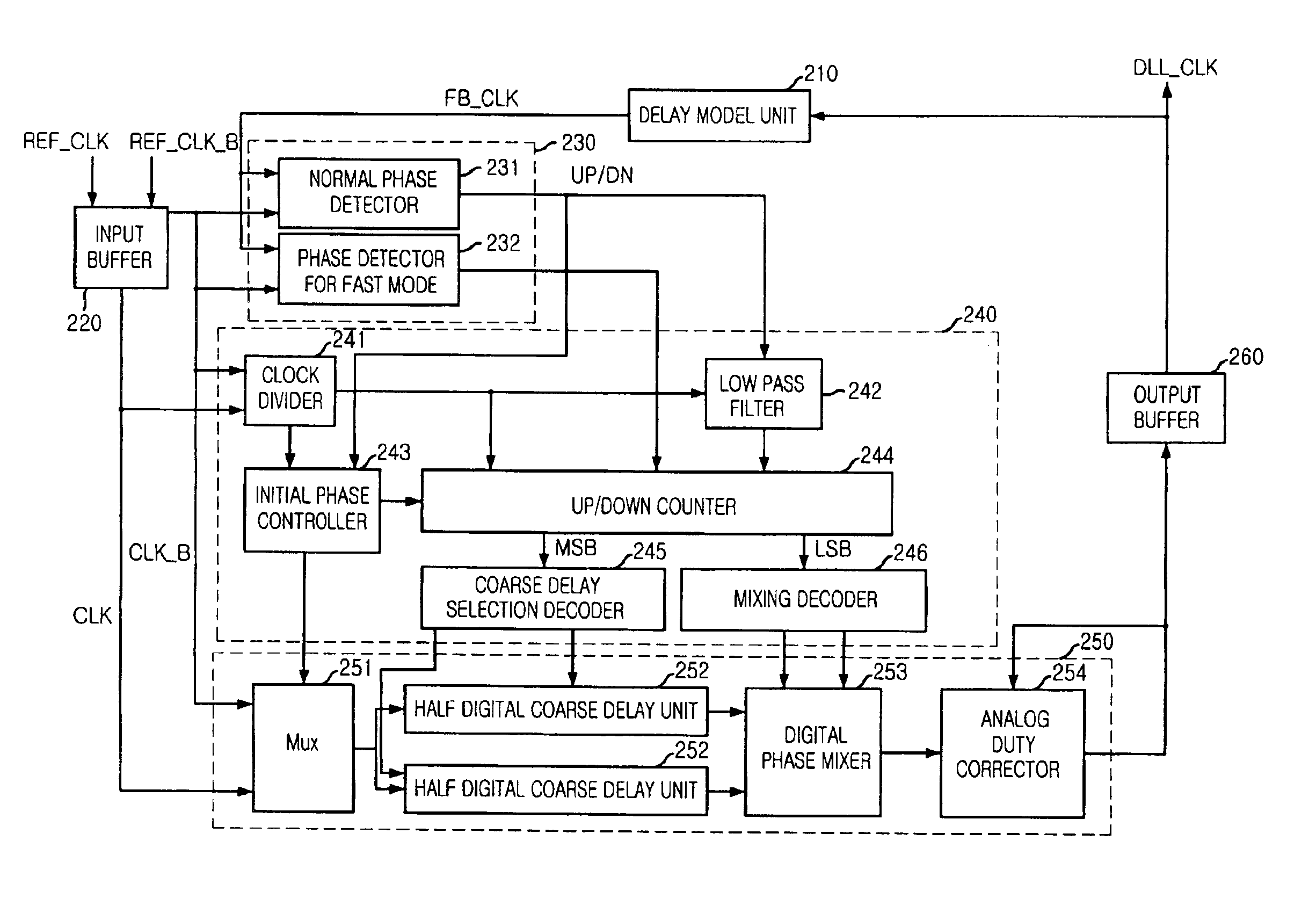
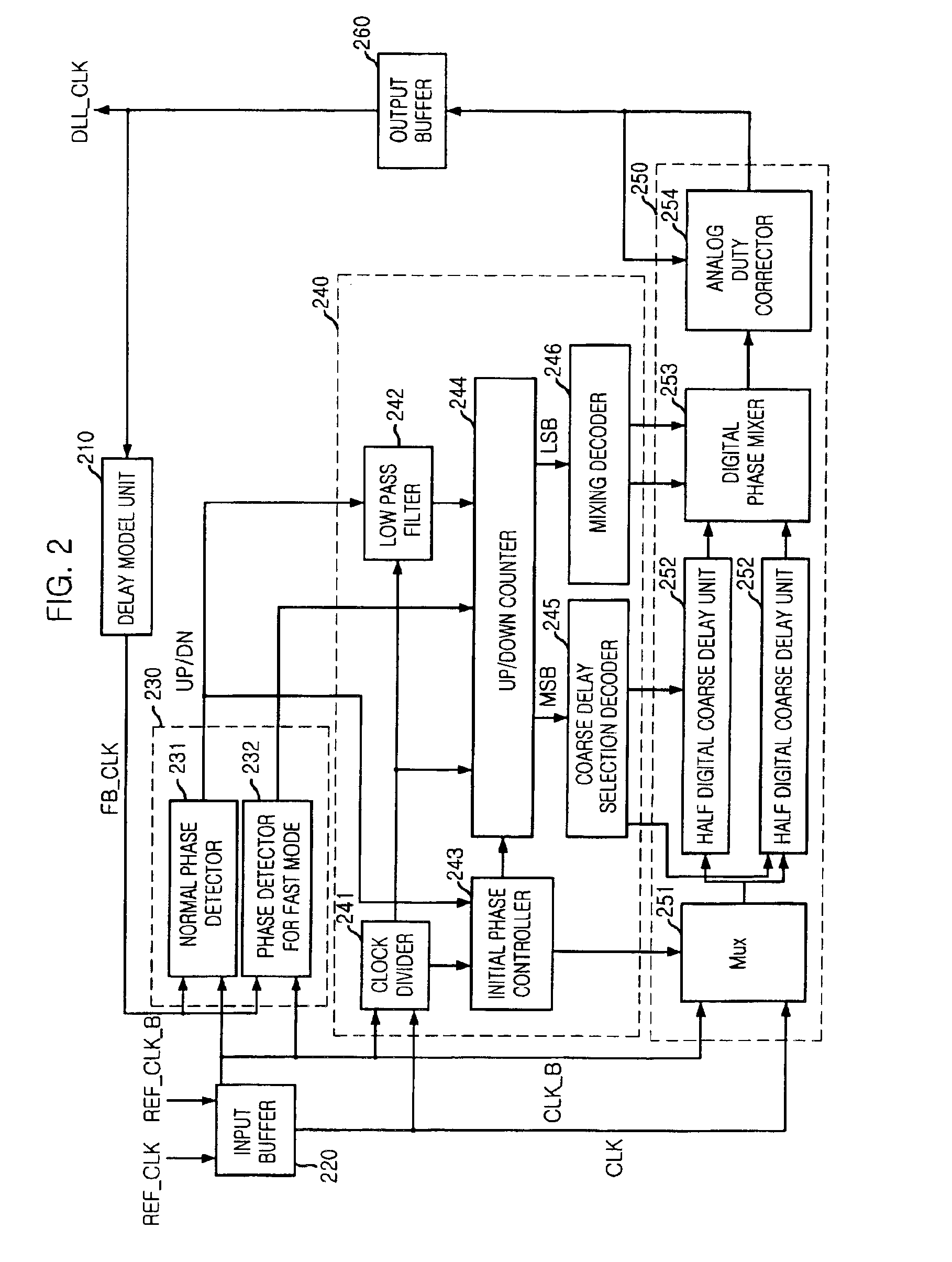
[0011]FIG. 2 is a block diagram illustrating a low jitter DLL circuit having a digital phase mixer in accordance with the preferred embodiment of the present invention. The DLL circuit includes a delay model unit 210, an input buffer 220, a phase detector 230, a controller 240 and a delay line unit 250.

[0012]The delay model unit 210 is used for compensating a time difference between a clock signal inputted from an external circuit and an internal clock signal substantially used in the system and outputs a compensation signal FB_CLK, and the compensation signal is inputted to the phase detector 230.

[0013]Also, the input buffer 220 receives a reference clock signal REF CLK and an inverted reference clock signal REF CLK B and gener...


PUM


Abstract

A DLL circuit having a low jitter in a semiconductor device, includes a delay model unit for compensating a time difference between an external clock signal and an internal clock signals and generating a compensation signal; an input buffer for receiving a reference clock signal and an inverted clock signal, and for outputting a clock signal and an inverted clock signal activated at each edges of the reference clock signal and the inverted clock signal; a phase detection unit for generating a comparison signal by comparing the compensation signal with the inverted clock signal, and for outputting the comparison signal with a normal mode or a fast mode; a control unit for generating a plurality of control signals by receiving the comparison signal, the inverted clock signal and the clock signal; a delay unit for delaying in response to the plurality of control signals; and an output buffer for outputting a delayed clock signal by receiving an output signal of the duty corrector.

Description

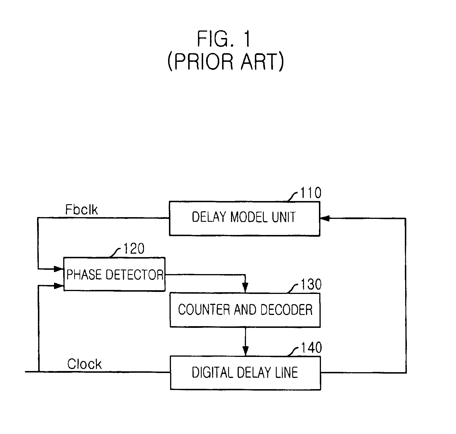
FIELD OF THE INVENTION[0001]The present invention relates to a semiconductor device; and, more particularly, to a delay locked loop circuit having a low jitter by using a digital phase mixer in the semiconductor device.DESCRIPTION OF RELATED ART[0002]Generally, a clock signal is employed to set a timing reference and secure a rapid operation without any error in a system or a circuit. At this time, a time delay is generated when the clock signal provided from the external circuit is used in an internal circuit. The time delay is adjusted by using a delay locked loop (DLL) circuit to synchronize the phase of the external clock signal with that of the internal clock signal.[0003]FIG. 1 is a block diagram showing a conventional DLL circuit. The conventional DLL circuit includes a delay model unit 110, a phase detector 120, a counter and decoder 130 and a digital delay line 140. The delay model unit 110 is used to compensate a time difference between an external clock signal and an inte...

Claims


Application Information

Patent Timeline
Patent Type & Authority Patents(United States)
IPC IPC(8): H03L7/087H03L7/081H03L7/08
CPCH03L7/0814H03L7/087H03L7/0816H03L7/0818H03L7/08
Inventor CHO, SEONG-IK
Owner SK HYNIX INC
Learn More