
Method of stabilizing material layer

a material layer and surface property technology, applied in vacuum evaporation coatings, chemical vapor deposition coatings, coatings, etc., can solve the problems of affecting the yield and stability of the semiconductor device, contaminating the untreated wafer surface, and dispersed wafers, so as to reduce the contamination on the wafer, reduce the increase of the resistance value due to oxidation, and improve the surface properties of the material layer on the wafer surface.

Inactive Publication Date: 2005-07-19
POWERCHIP SEMICON MFG CORP
View PDF11 Cites 5 Cited by
  • Summary
  • Abstract
  • Description
  • Claims
  • Application Information

AI Technical Summary

Benefits of technology

[0007]Accordingly, it is an object of the present invention to provide a method of stabilizing material layers, wherein wafers are stored in the FOUP filled with gas to stabilize the properties of the material layers on the wafer, avoiding inconsistency of properties of the surface of individual wafers as a result of the difference caused by oxidation.
[0008]Yet another object of the present invention is to provide a method of stabilizing a material layer, wherein the wafers with deposited a material layer are stored in a FOUP filled with gas so as to reduce outgassing as a result of the residual gas on the wafer, avoiding the outgassing contamination of the untreated wafer in the FOUP.
[0009]The present invention provides a method of stabilizing material layers by transferring a wafer to a chamber to form a material layer, wherein the material of the material layer is selected from the group consisting of metal, metal nitrides, metal silicides or oxides. Next, the wafer deposited with material layer is transferred to a FOUP filled with gas for storage, wherein the filled gas is, for example inert gas or oxygen. When an inert gas is used to fill the FOUP, the oxidizing situation on the wafer surface can be retarded, and the increased resistance value due to oxidation can be reduced such that the surface properties of the material layer on the wafer surface are more stable. By way of purging with nitrogen, the deposited reacting residual gas from the FOUP is removed so as to lower contamination on the wafer as a result of outgassing. Besides, when oxygen is filled in the FOUP, the extent of oxidation of the material layer surface is increased such that the resistance value becomes greater. Thus, the stability of the surface properties of the wafer in the FOUP is increased. Of course, by means of purging with oxygen, the reacting residual gas will be discharged from the FOUP so as to reduce contamination on other wafers as a result of outgassing.

Problems solved by technology

Such a difference affects the subsequent fabrication process to a certain extent, and consequently the yield and stability of the semiconductor device will be affected.
This gas dispersed from the wafer will contaminate the untreated wafer surface.

Method used


Image

  • Method of stabilizing material layer
  • Method of stabilizing material layer

Examples


Embodiment Construction

[0018]Reference will now be made in detail of the present preferred embodiments of the invention, examples of which are illustrated in the accompanying drawings. Wherever possible, the same reference numbers are used in the drawings and the description to refer to the same or like parts.

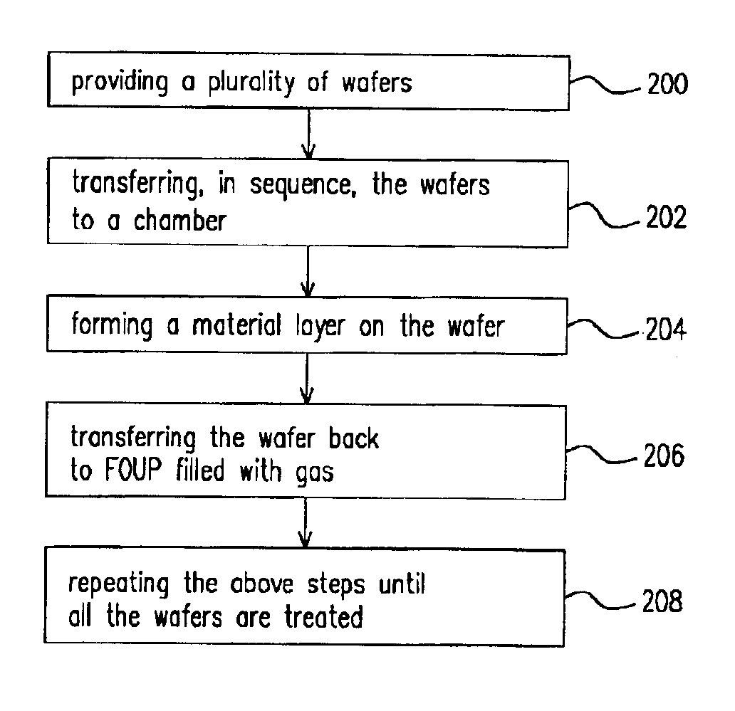
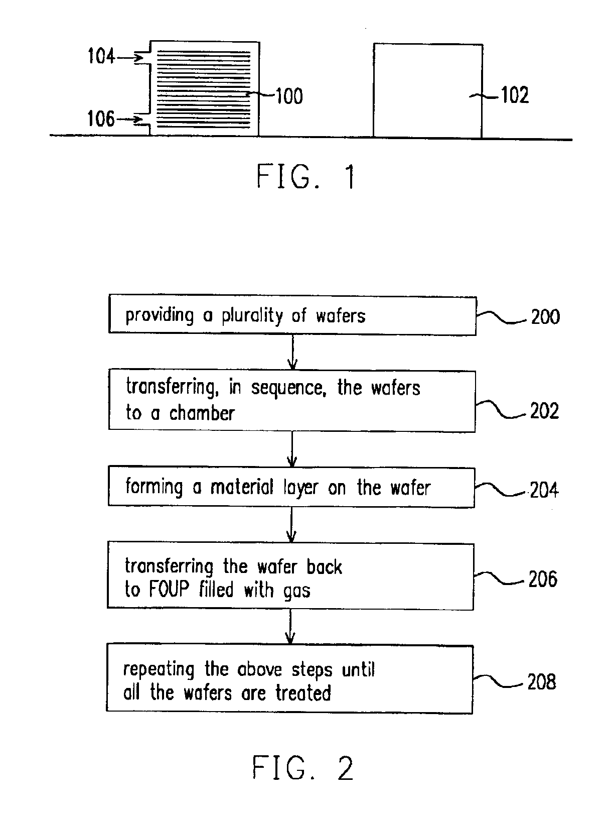
[0019]FIG. 1 schematically shows a fabrication device for forming of the material layer of a preferred embodiment of the present invention. FIG. 2 is a flowchart showing a method of forming a material layer of the preferred embodiment in accordance with the present invention.

[0020]Referring to FIGS. 1 and 2, step 200 indicates the step of providing a plurality of wafers, and the wafers are kept in the FOUP 100. An example of a FOUP 100 is the FOUP that can store 25 wafers. After that, a robot blade is used to respectively transfer the wafers from the FOUP 100 to a chamber (step 202). In other words, the wafers in the FOUP 100 are transferred, one-by-one, to the chamber 102 to proceed with reaction. T...


PUM

PropertyMeasurementUnit
Electrical resistanceaaaaaaaaaa
Surface propertiesaaaaaaaaaa

Abstract

A method of stabilizing the properties of a material layer is disclosed. A plurality of wafers are stored in a FOUP and in sequence the wafers are transferred to a chamber to proceed with deposition of a material layer and to the FOUP filled with a specific gas after deposition until all the wafers in the FOUP are treated. In the process of deposition, the wafers deposited with material layers on their surfaces are stored in the FOUP filled with specific gas. Therefore, the surface properties of all the wafers in the FOUP are stablilized and contamination due to outgassing is prevented.

Description

BACKGROUND OF INVENTION[0001]1. Field of the Invention[0002]The present invention relates to a method of manufacture for a semiconductor device, particularly a method of stabilizing surface properties of a material layer.[0003]2. Description of the Related Art[0004]Film deposition is one of the important steps in semiconductor device fabrication process. Generally, a semiconductor device is constituted from a plurality of layers (material layers) of films of various thickness. The stability of these films (material layers) will affect the performance of the semiconductor device. Therefore, in semiconductor fabrication process, how to stabilize the surface properties of the material layers is important.[0005]For instance, in general, in the process of depositing material layers, a plurality of wafers are stacked and placed in a Front Opening Unified Pod, FOUP. A robot arm is used to take the wafers, in sequence, from the FOUP and transfer the wafers to a chamber to proceed with the d...

Claims


Application Information

Patent Timeline
IPC IPC(8): C23C16/22C23C16/34C23C14/56C23C16/44C23C16/54
CPCC23C14/564C23C16/4408C23C16/54
Inventor CHEN, CHING-HUA
Owner POWERCHIP SEMICON MFG CORP
Features
  • Generate Ideas
  • Intellectual Property
  • Life Sciences
  • Materials
  • Tech Scout
  • Unparalleled Data Quality
  • Higher Quality Content
  • 60% Fewer Hallucinations
Learn More