Semiconductor part of component mounting, mounting structure and mounting method

a semiconductor and component technology, applied in the direction of printed circuit aspects, sustainable manufacturing/processing, final product manufacturing, etc., can solve the problems of increasing the surface mounting density of the semiconductor components used in the above devices, increasing the size of supposedly small csp (chip scale packages), and increasing the scope of the area terminal layout. , to achieve the effect of reducing board wiring costs, increasing the number of pins, and facilitating mounting

Inactive Publication Date: 2005-07-19
SONY CORP
View PDF5 Cites 13 Cited by
  • Summary
  • Abstract
  • Description
  • Claims
  • Application Information

AI Technical Summary

Benefits of technology

[0025]The pitch array becomes finer (smaller) the more the area terminal is positioned on the inner side away from the outer circumferential side so that the number of terminals can be increased and the board is able to cope with recent and future trends towards increased numbers of pins.
[0026]The larger pitch array of the area terminals close to the outer circumference further signifies that the wiring circumferential terminals has an ample margin and that easier mounting and lower board wiring costs can be achieved. The larger pitch array also means larger wires (or wiring) can be utilized so that high-speed, high frequency mounting can be achieved since losses due to resistance in the wiring are reduced.

Problems solved by technology

Therefore, to what extent the surface mounting density of the semiconductor components used in the above devices can be increased has become an important technical issue.
However, to cope with semiconductor LSI chips having higher density and more functions, the scope of the area terminal layout has shown a tend to continually increase and even the size of supposedly small CSP (chip scale packages) are becoming larger.
However, when miniaturizing the pitch array of area terminals in this way, reducing the size of the terminals is of course unavoidable.
Even when mounting (connecting) chip scale packages (CSP) on boards, there is a large possibility of the connection strength deteriorating due to factors such as heat stress after mounting.
Thus, when many wires are laid between the area terminals and the gap between the terminals becomes exceedingly small, then fine complex processing also becomes necessary on the board.

Method used


Image

  • Semiconductor part of component mounting, mounting structure and mounting method
  • Semiconductor part of component mounting, mounting structure and mounting method
  • Semiconductor part of component mounting, mounting structure and mounting method

Examples


Embodiment Construction

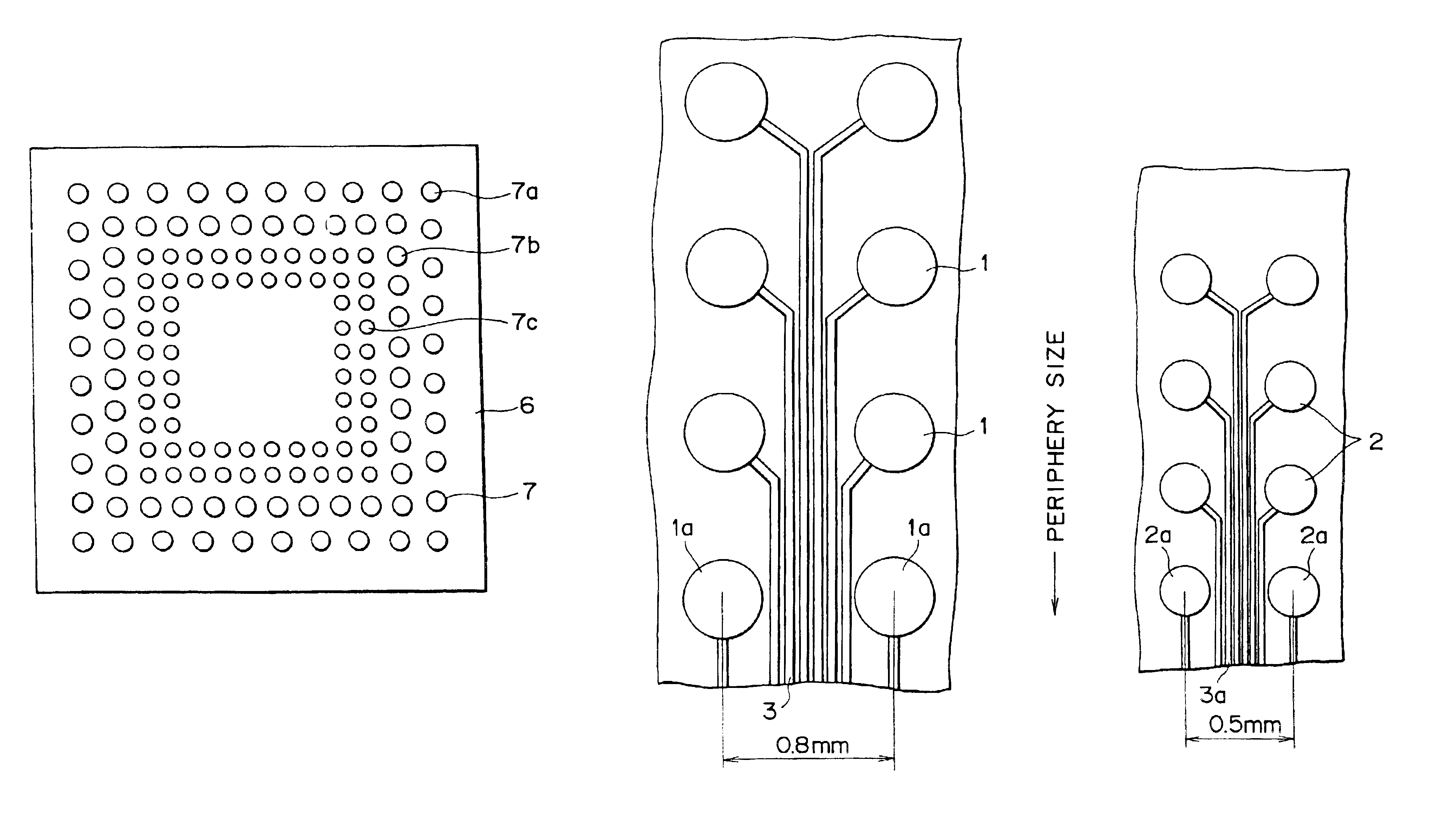
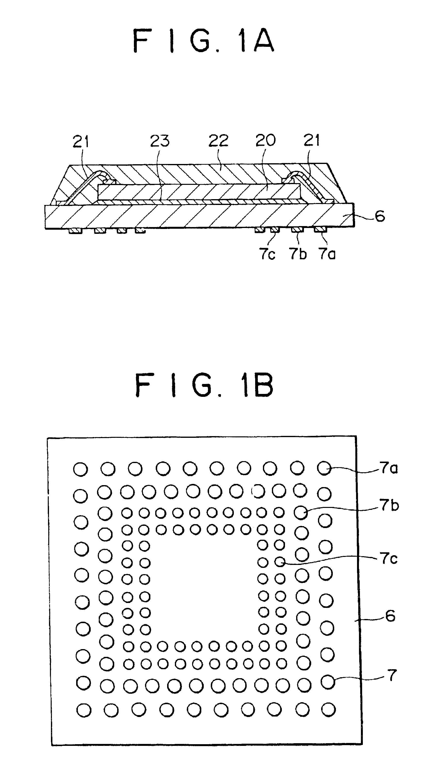
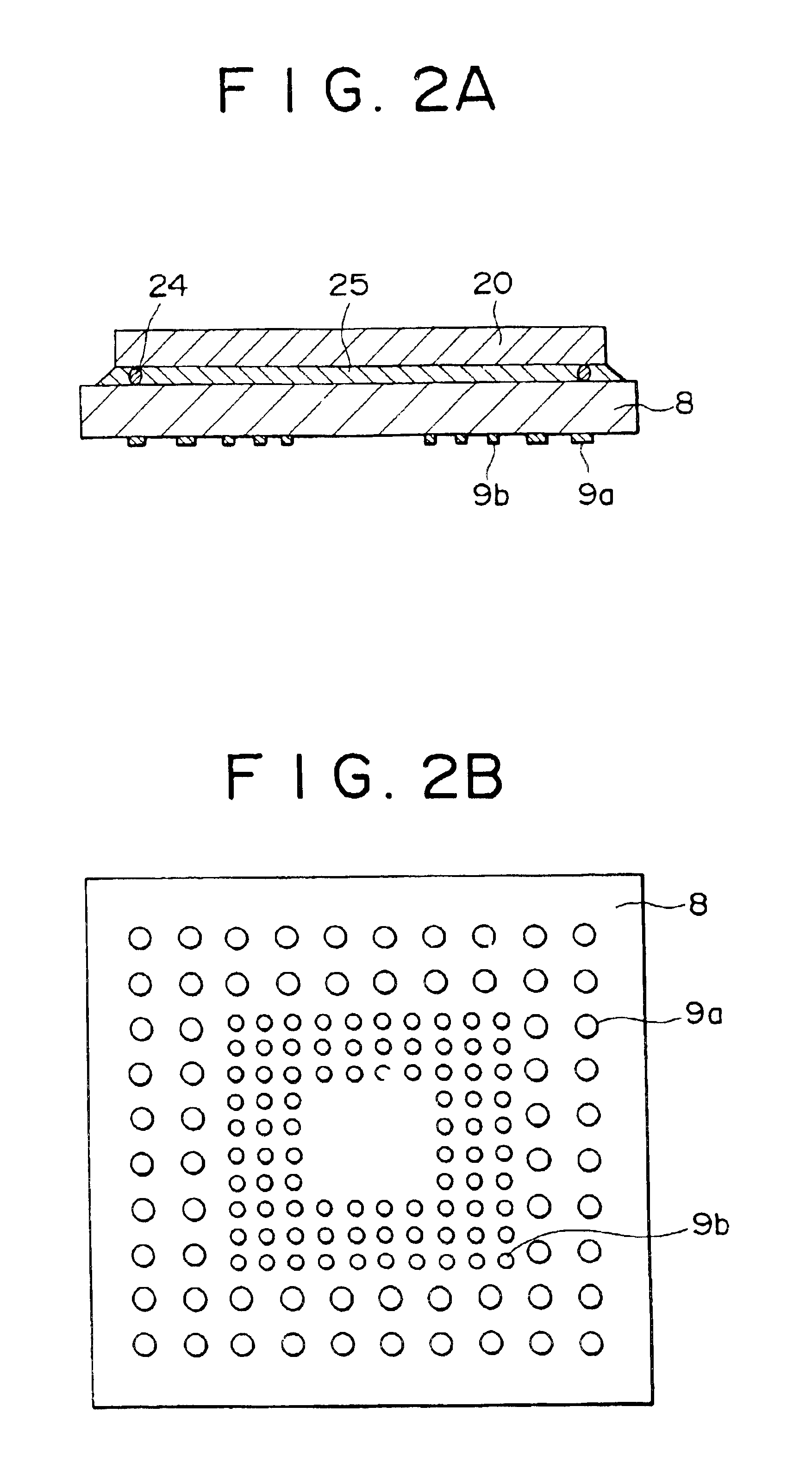
[0035]The preferred embodiments of this invention will now be described in specific detail while referring to the accompanying drawings. The scope of this invention is not however limited by such drawings or descriptions. pitch of 0.8 mm are positioned on the outer circumference of an interposer board 6 of the CSP as shown in FIGS. 1A and 1B. On the inner side of the area terminal 7 row is one row of mid-size area terminals 7b at a pitch of 0.65 mm and still further towards the inside of the interposer board 6 are two rows of small area terminals 7c arrayed at a pitch of 0.5 mm. In FIG. 1A, the reference numeral 20 denotes an LSI (large scale integrated circuit) chip, 21 is bonding wires, 22 is a plastic molded package, and 23 is a bonding solution (adhesive). The total number of area terminals 7 in this state is 136 pins. In contrast, in the conventional arrangement of area terminals all of the same diameter arrayed at a 0.8 mm pitch, the total number of area pins does not exceed 9...


PUM


Abstract

A semiconductor part for component mounting, a mounting structure and a mounting method providing ample surplus wiring pitch and width between terminals in order to improve the strength of the connection with the printed circuit board in view of the recent trends towards a greater number of pins and greater component mounting density on printed circuit boards or substrates. A semiconductor component for mounting has area terminals comprised of area terminals mounted on the outer circumferential side and area terminals mounted on the inner circumferential side of the board. The area terminals on the outer circumferential side of the board are arranged with a larger pitch and or diameter than the area terminals on the inner circumferential side. A mounting method and mounting structure having land terminals arrayed on a printed circuit board or substrate with the same arrangement as the area terminals of the semiconductor component, and the land terminals are connected with the area terminals by a conductive bonding agent.

Description

CROSS REFERENCE TO RELATED APPLICATIONS[0001]This application is a divisional Patent Application under 37 CFR 1.53(b) based on Parent application Ser. No. 09 / 398,100, filed Sep. 17, 1999 now U.S. Pat. No. 6,534,875 which claims priority to Japanese Application No. P10-271740, filed Sep. 25, 1998.BACKGROUND OF THE INVENTION[0002]1. Field of the Invention[0003]The present invention relates to a semiconductor part for component mounting, a mounting structure and a mounting method.[0004]2. Description of Related Art[0005]Strong demands have been made in recent years for portable electronic equipment such as digital cameras, digital portable telephones and notebook type personal computers that are thinner, are more compact and have lighter weight. Therefore, to what extent the surface mounting density of the semiconductor components used in the above devices can be increased has become an important technical issue.[0006]To cope with this trend, the development of compact CSP (chip scale ...

Claims


Application Information

Patent Timeline
Patent Type & Authority Patents(United States)
IPC IPC(8): H01L23/498H01L23/48H05K3/34H05K1/11H01L23/12H01L21/60
CPCH01L23/49838H05K3/3436H01L2224/48227H01L2924/15311H05K1/111H05K2201/094H05K2201/10734H05K2203/0465H01L24/48H01L2224/05599H01L2224/73265H01L2224/85399H01L2924/00014H01L2924/14H01L2924/181Y02P70/50H01L2924/00012H01L2224/45015H01L2924/207H01L2224/45099H01L2924/00H01L23/12H01L21/60
Inventor NISHIYAMA, KAZUO
Owner SONY CORP
Why Eureka
Try Eureka