Process for producing semiconductor article using graded epitaxial growth

a technology of epitaxial growth and semiconductors, applied in the direction of semiconductor devices, basic electric elements, electrical apparatus, etc., can solve the problems of limiting the maximum ge composition to a low value, complicating or destroying the silicon layer may also complicate or undermine the performance of devices built, so as to achieve simplified and improved process, high quality material

Inactive Publication Date: 2005-07-26
MASSACHUSETTS INST OF TECH
View PDF305 Cites 49 Cited by
  • Summary
  • Abstract
  • Description
  • Claims
  • Application Information

AI Technical Summary

Benefits of technology

[0010]According to the invention, there is provided an improved technique for production of wide range of high quality material is provided. In particular, the production of relaxed Si1-xGex-on-insulator (SGOI) substrate or relaxed III-V or II-VI material-on-insulator, such as GaAs-on-insulator, is described. High quality monocrystalline relaxed SiGe layer, relaxed Ge layer, or other relaxed III-V material layer is grown on a silicon substrate using a graded Si1-xGex epitaxial growth technique. A thin film of the layer is transferred into an oxidized handle wafer by wafer bonding and wafer splitting using hydrogen ion implantation. The invention makes use of the graded Si1-xGex buffer structure, resulting in a simplified and improved process.
[0011]The invention also provides a method allowing a wide range of device materials to be integrated into the inexpensive silicon substrate. For example, it allows production of Si1-xGex-on-insulator with wide range of Ge concentration, and allows production of many III-V or II-VI materials on insulator like GaAs, AlAs, ZnSe and InGaP. The use of graded Si1-xGex buffer in the invention allows high quality materials with limited dislocation defects to be produced and transferred. In one example, SGOI is produced using a SiGe structure in which a region in the graded buffer can act as a natural etch stop.

Problems solved by technology

One of the main drawbacks is the quality of the resulting Si1-xGex film and BOX.
In addition, Ge segregation during high temperature anneal also limits the maximum Ge composition to a low value.
The silicon layer in the structure is unnecessary, and may complicate or undermine the performance of devices built on it.
For example, it may form a parasitic back channel on this strained-Si, or may confine unwanted electrons due to the band gap offset between the strained-Si and SiGe layer.
The presence of the silicon layer in the above structure may be for the purpose of facilitating Si-insulator wafer bonding, but is unnecessary for ideal SGOI substrates.
Again, the silicon layer may also complicate or undermine the performance of devices built on it.
For example, it may form a parasitic back channel on this strained-Si, or may confine unwanted electrons due to the band gap offset between the strained-Si and SiGe layer.
Moreover, the etch stop of P++ in the above structure is not practical when the first graded Si1-yGey layer described in the patents has a y value of larger than 0.2.
Therefore, the KOH will not be able to remove the first graded Si1-yGey layer and the second relaxed SiGe layer as described in the patents.
Other attempts include re-crystallization of an amorphous Si1-xGex layer deposited on the top of SOI (silicon-on-insulator) substrate, which is again not an ideal SGOI substrate and the silicon layer is unnecessary, and may complicate or undermine the performance of devices built on it.

Method used


Image

  • Process for producing semiconductor article using graded epitaxial growth
  • Process for producing semiconductor article using graded epitaxial growth
  • Process for producing semiconductor article using graded epitaxial growth

Examples


Embodiment Construction

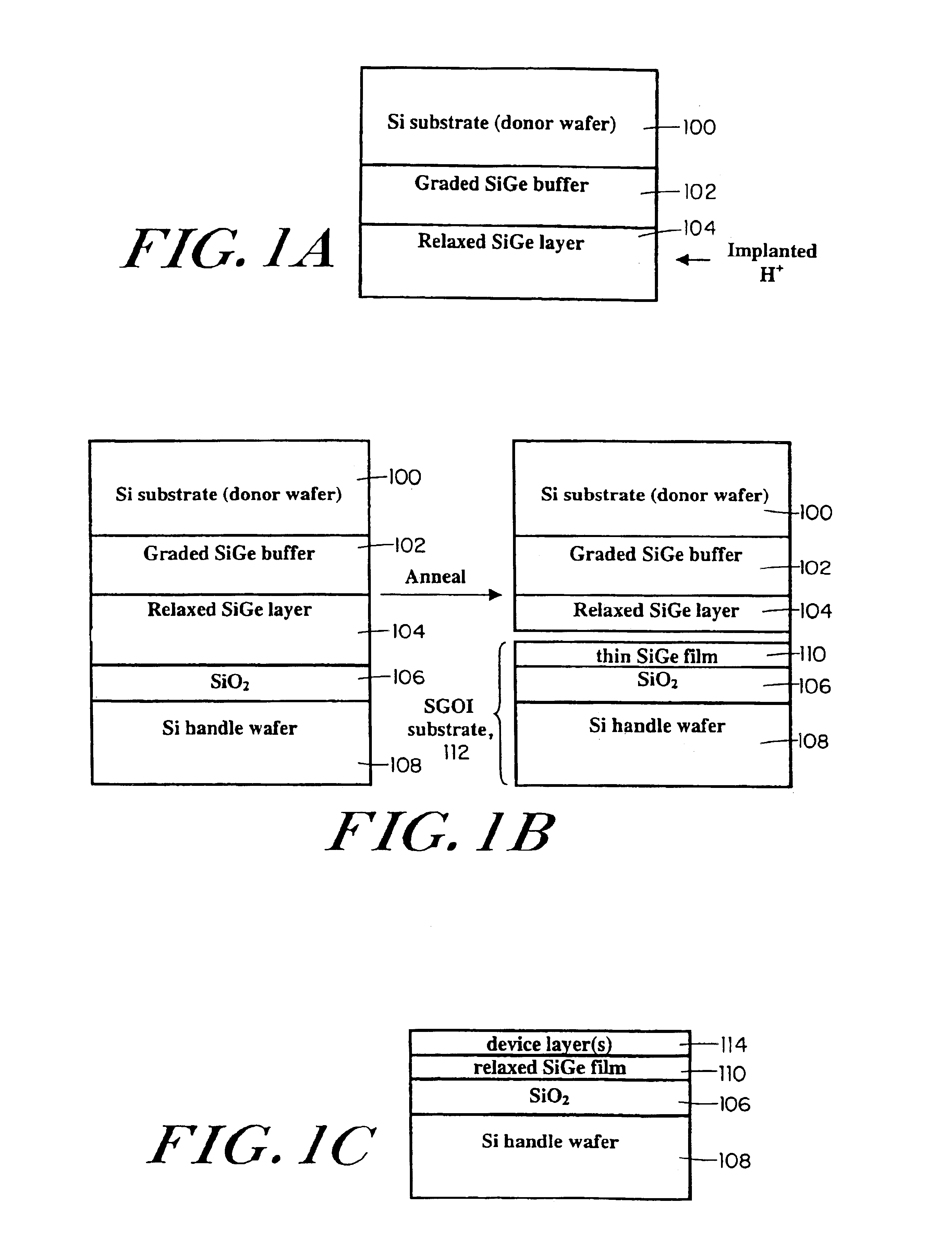
[0019]An example of a process in which SGOI is created by layer transfer is described. The experiment was performed in two stages. In the first stage, heteroepitaxial SiGe layers are formed by a graded epitaxial growth technology. Starting with a 4-inch Si (100) donor wafer 100, a linearly stepwise compositionally graded Si1-xGex buffer 102 is deposited with CVD, by increasing Ge concentration from zero to 25%. Then a 2.5 μm relaxed Si0.75Ge0.25 cap layer 104 is deposited with the final Ge composition, as shown in FIG. 1A.

[0020]The relaxed SiGe cap layer has high quality with very low dislocation defect density (less than 1E6 / cm2), as the graded buffer accommodates the lattice mismatch between Si and relaxed SiGe. A thin layer of this high quality SiGe will be transferred into the final SGOI structure. The surface of the as-grown relaxed SiGe layer shows a high roughness around 11 nm to 15 nm due to the underlying strain fields generated by misfit dislocations at the graded layer in...


PUM

PropertyMeasurementUnit
surface roughnessaaaaaaaaaa
temperatureaaaaaaaaaa
roughnessaaaaaaaaaa

Abstract

A process for producing monocrystalline semiconductor layers. In an exemplary embodiment, a graded Si1-xGex (x increases from 0 to y) is deposited on a first silicon substrate, followed by deposition of a relaxed Si1-yGey layer, a thin strained Si1-zGez layer and another relaxed Si1-yGey layer. Hydrogen ions are then introduced into the strained SizGez layer. The relaxed Si1-yGey layer is bonded to a second oxidized substrate. An annealing treatment splits the bonded pair at the strained Si layer, such that the second relaxed Si1-yGey layer remains on the second substrate. In another exemplary embodiment, a graded Si1-xGex is deposited on a first silicon substrate, where the Ge concentration x is increased from 0 to 1. Then a relaxed GaAs layer is deposited on the relaxed Ge buffer. As the lattice constant of GaAs is close to that of Ge, GaAs has high quality with limited dislocation defects. Hydrogen ions are introduced into the relaxed GaAs layer at the selected depth. The relaxed GaAs layer is bonded to a second oxidized substrate. An annealing treatment splits the bonded pair at the hydrogen ion rich layer, such that the upper portion of relaxed GaAs layer remains on the second substrate.

Description

PRIORITY INFORMATION[0001]This application is a continuation of application Ser. No. 10 / 384,160, filed Mar. 7, 2003, now U.S. Pat. No. 6,737,670 that is a divisional of application Ser. No. 09 / 928,126, filed on Aug. 10, 2001, issued as U.S. Pat. No. 6,573,126 on Jun. 3, 2003, which claims priority from provisional application Ser. No. 60 / 225,666, filed Aug. 16, 2000, now expired, the entire disclosures of which are incorporated by reference herein.BACKGROUND OF THE INVENTION[0002]The present invention relates to a production of a general substrate of relaxed Si1-xGex-on-insulator (SGOI) for various electronics or optoelectronics applications, and the production of monocrystalline III-V or II-VI material-on-insulator substrate.[0003]Relaxed Si1-xGex-on-insulator (SGOI) is a very promising technology as it combines the benefits of two advanced technologies: the conventional SOI technology and the disruptive SiGe technology. The SOI configuration offers various advantages associated wi...

Claims


Application Information

Patent Timeline
Patent Type & Authority Patents(United States)
IPC IPC(8): H01L21/762H01L21/20H01L21/02H01L21/70H01L27/12H01L21/205
CPCH01L21/02381H01L21/0245H01L21/02502H01L21/0251H01L21/02521H01L21/02532H01L21/02546H01L21/76254Y10S438/933
Inventor CHENG, ZHI-YUANFITZGERALD, EUGENE A.ANTONIADIS, DIMITRI A.HOYT, JUDY L.
Owner MASSACHUSETTS INST OF TECH
Why Eureka
Try Eureka