

Use of gate electrode workfunction to improve DRAM refresh
a gate electrode and workfunction technology, applied in semiconductor devices, digital storage, instruments, etc., can solve the problems of increasing the doping level of the underlying channel region of the substrate, increasing current leakage, and aggravated efforts to alleviate one leakage problem, so as to reduce the doping requirements of the array substrate channel region, reduce and minimize the effect of transistor and diode current leakag
- Summary
- Abstract
- Description
- Claims
- Application Information
AI Technical Summary
Benefits of technology
Problems solved by technology
Method used
Image

Examples
embodiment 1
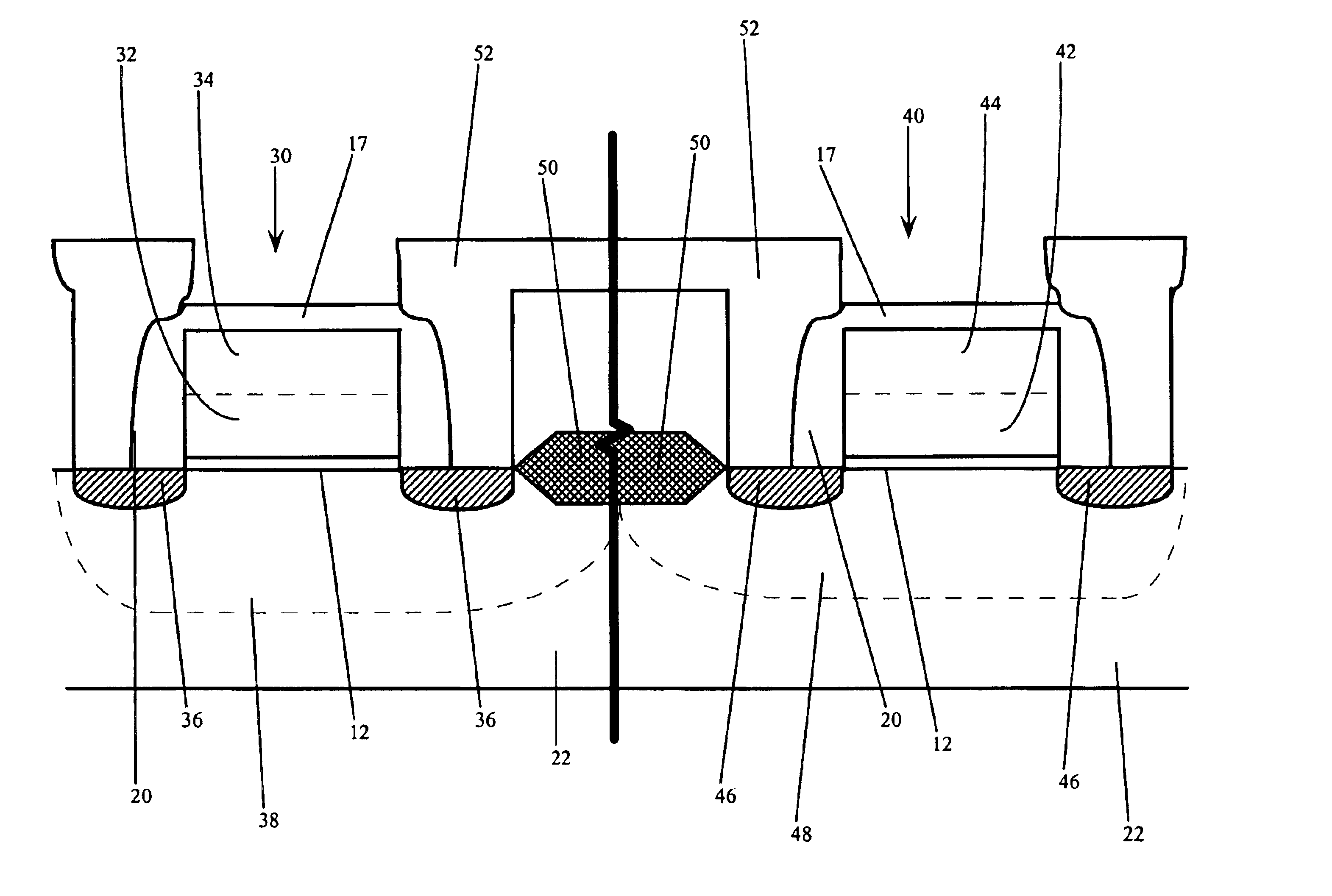
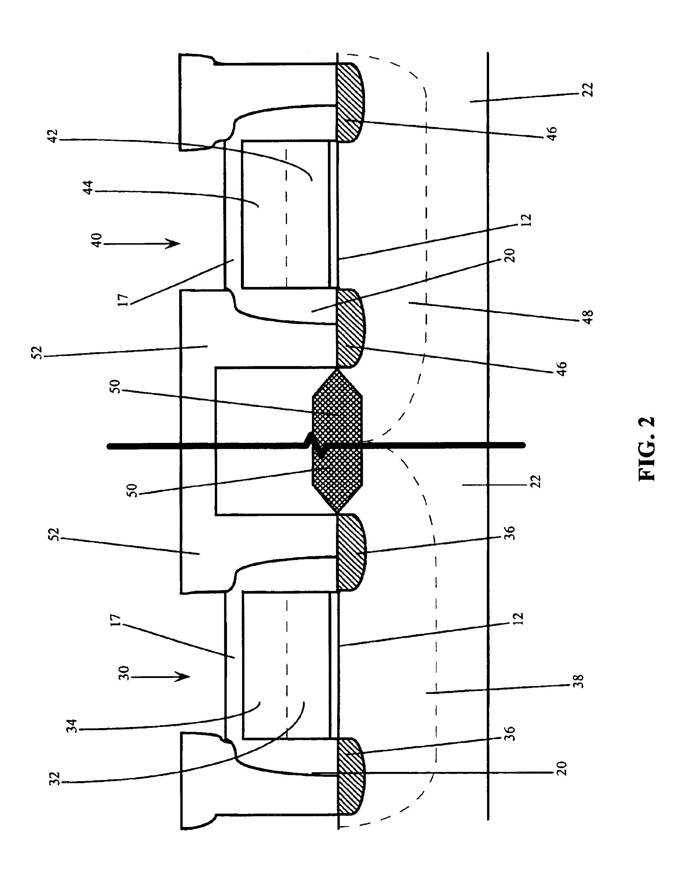
[0037]In the first embodiment, the semiconductor device structure has access transistors comprising P+ Si / Ge gate electrodes 14, periphery NMOS transistors comprising P+ Si / Ge gate electrodes 32 and periphery PMOS transistors comprising P+ Si / Ge gate electrodes 42.
embodiment 2
[0038]In the second embodiment, the semiconductor device structure has access transistors comprising P+ Si / Ge gate electrode 14, a majority of periphery NMOS transistors comprise N+ Si / Ge gate electrodes 32, and a minority of periphery NMOS transistors comprise P+ Si / Ge gate electrodes 32, and a majority of the periphery PMOS transistors comprise P+ Si / Ge gate electrode 42, and a minority comprise N+ Si / Ge gate electrodes 42.
embodiment 3
[0039]For the third embodiment, the semiconductor device structure has access transistors comprising either N+ or P+ Si / Ge gate electrodes 14, a majority of periphery NMOS transistors comprise a N+ poly gate electrodes 32, and may have a minority comprise either P+ poly or Si / Ge gate electrodes 32, and periphery PMOS transistors comprise either P+ poly or N+ poly gate electrodes 42.
PUM
 Abstract
Description
Claims
Application Information