Self-aligned gate formation using polysilicon polish with peripheral protective layer

Inactive Publication Date: 2005-08-02
GLOBALFOUNDRIES INC
View PDF1 Cites 13 Cited by
  • Summary
  • Abstract
  • Description
  • Claims
  • Application Information

AI Technical Summary

Benefits of technology

[0012]It is therefore an object of this invention to provide a method for minimizing polysilicon dishing

Problems solved by technology

The aforementioned self-aligned poly gate process using poly CMP has great potential for improving density of flash memory circuits, but has not been successfully implemented in manufacturing of flash memory due to associated problems.
The dishing effect can cause severe

Method used


Image

  • Self-aligned gate formation using polysilicon polish with peripheral protective layer
  • Self-aligned gate formation using polysilicon polish with peripheral protective layer
  • Self-aligned gate formation using polysilicon polish with peripheral protective layer

Examples


Example

[0027]A first embodiment of our invention utilizes a protective mask 35 which is patterned to be slightly smaller than the large surface active silicon areas in the peripheral region 31, as illustrated in FIG. 4a. A second embodiment of our invention utilizes a protective mask 35′ which is patterned to be larger than the active silicon areas 36 in the peripheral region 31, as illustrated in FIG. 4b.

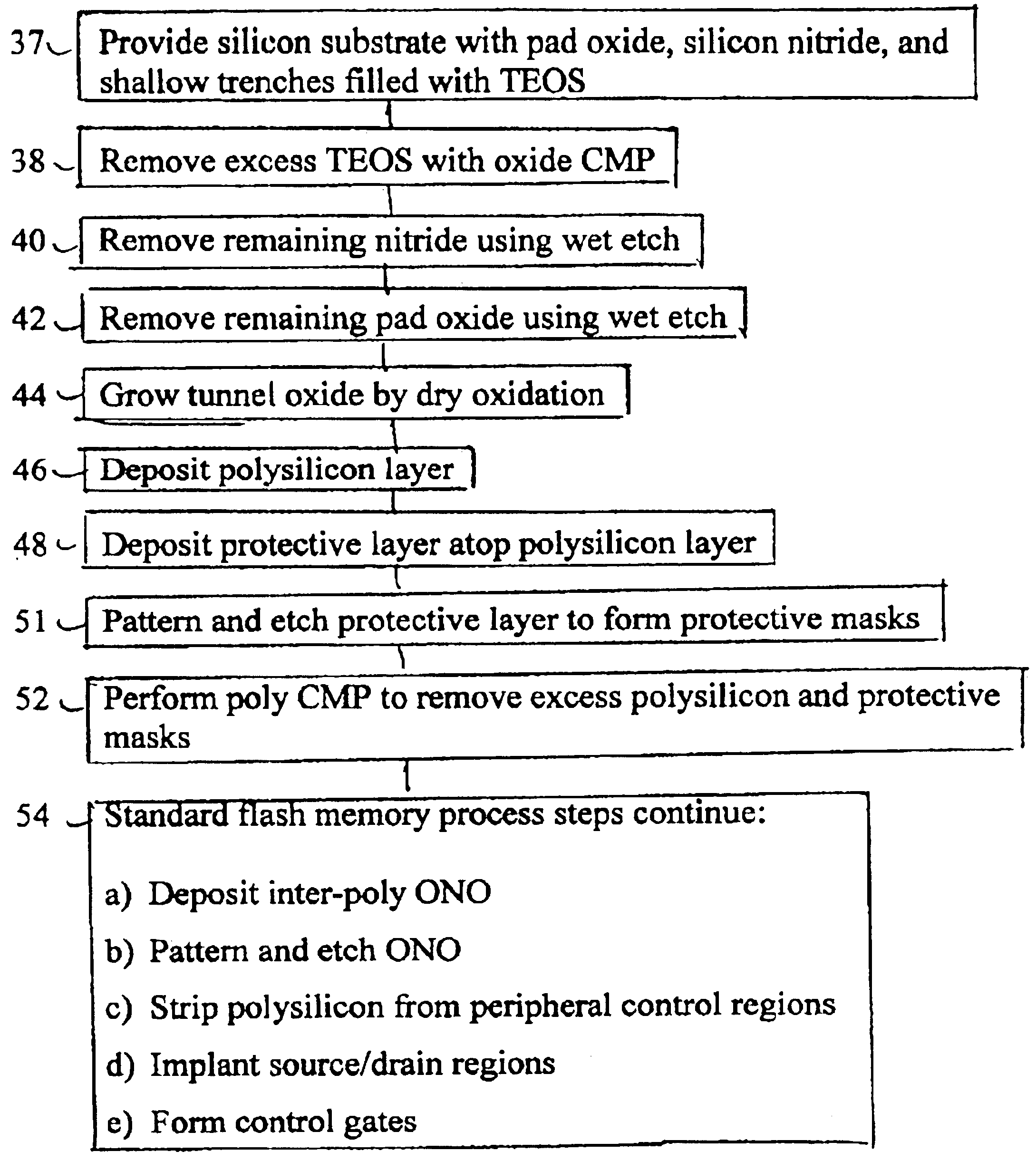
[0028]FIG. 5 is a process flow chart which incorporates the protective layers shown in FIGS. 4a and 4b.

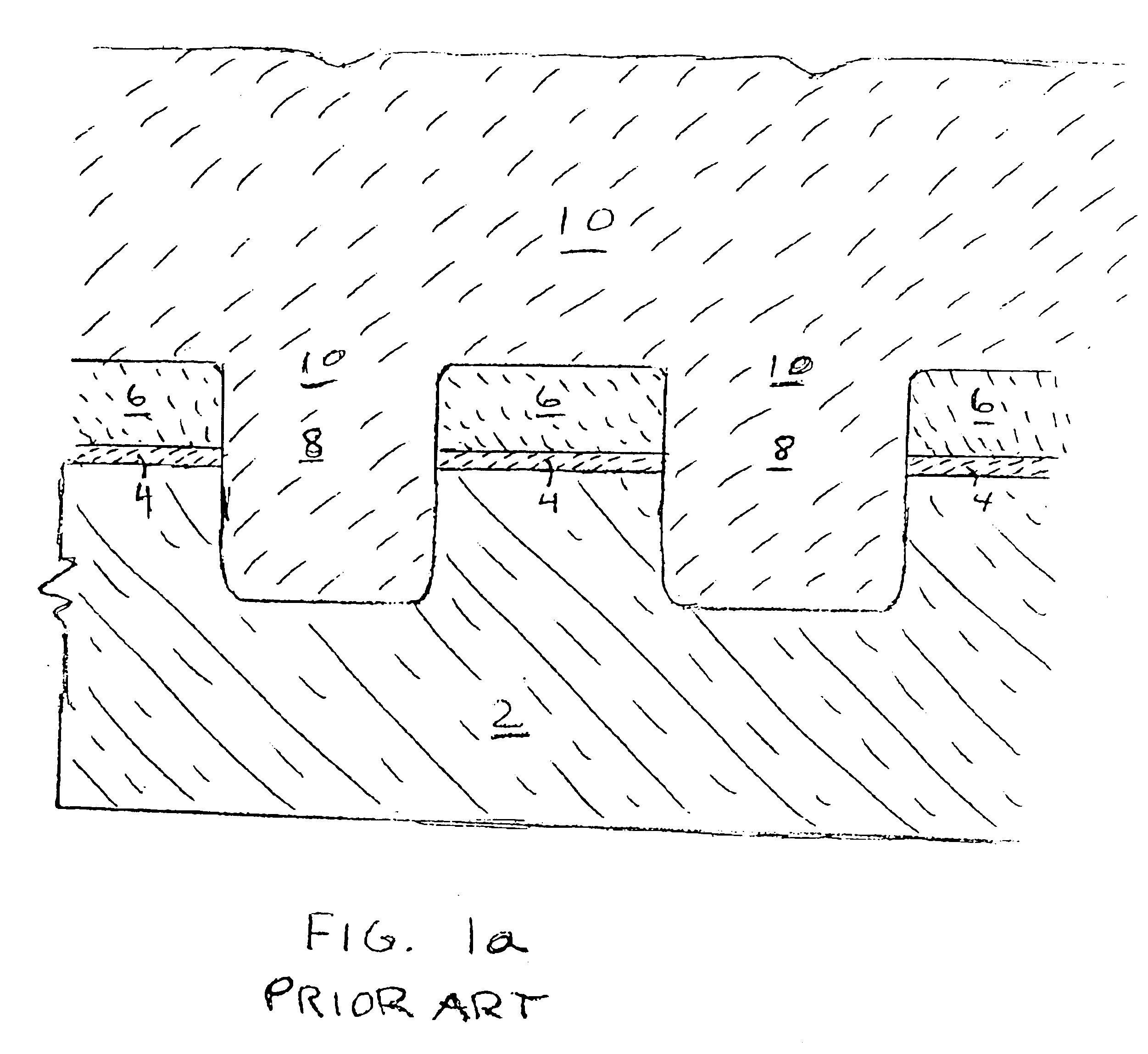
[0029]In step 37, a silicon substrate 2 is provided having pad oxide 4 thereon, having silicon nitride layer 6 atop pad oxide 4, and having etched shallow trenches 8 filled with TEOS 10.

[0030]In step 38, oxide CMP is performed to remove excess TEOS atop nitride layer 6, stopping on nitride layer 6.

[0031]In step 40, remaining nitride layer 6 is removed using wet etch techniques.

[0032]In step 42, remaining pad oxide 4 is removed using wet etch techniques.

[0033]In step 44, tunnel oxide la...

Example

[0046]FIG. 6b illustrates the second embodiment of our inventive process after polysilicon CMP. The patterned protective mask 35′ as shown in FIG. 4b is utilized to provide protection for underlying polysilicon over not only the peripheral active silicon regions 36, but also over the peripheral trench isolation regions 60. The protective mask covers substantially the entire peripheral area of the chip, with an opening window which leaves the central memory cell array with small feature sizes uncovered. To prevent residual polysilicon film atop the edge 62 of the memory cell array, the opening window of the protective mask is made larger than the memory cell array, typically 5 to 30 microns larger. Advantages of this second embodiment of the patterned protective mask include simple lithography with non-critical alignment, as well as prevention of thinning of trench oxide and possible opening or enlarging of the trench seam during ONO overetch. The possible non-planar topography at co...


PUM


Abstract

A method of protecting a peripheral region, by forming a protective mask over the peripheral area, during polysilicon polishing while forming self-aligned polysilicon gates in flash memory circuits. In one aspect, the protective mask is formed over a substantial area of the Peripheral region. In another aspect, the protective mask is formed over a substantial area of an active part of the peripheral region.

Description

CROSS REFERENCE TO RELATED APPLICATION[0001]This application is related to the concurrently filed application Ser. No. 09 / 922,354, entitled “Insertion of Dummy Trenches to Avoid Silicon Damage for Self Aligned Polygate Process”.FIELD OF THE INVENTION[0002]This invention deals with integrated circuit manufacturing processes, and in particular to a process for forming a self-aligned gate for flash memory application using polysilicon polish.BACKGROUND OF THE INVENTION[0003]Self-aligned gate formation is desirable in integrated circuit fabrication processes. Use of self-aligned gates avoids problems caused by lithography misalignment, which become increasingly severe when critical dimensions are pushed below 0.18 microns. Critical dimension control is also improved by use of self-aligned gates.[0004]A process for forming a self-aligned gate for a floating gate device is illustrated in FIGS. 1a-1d. [0005]FIG. 1a shows silicon substrate 2 with pad oxide 4 generally of thickness 100-200 A...

Claims


Application Information

Patent Timeline
IPC IPC(8): H01L21/321H01L21/8247H01L27/105
CPCH01L21/3212H01L27/105H01L27/11526H01L27/11531H10B41/42H10B41/40
Inventor YANG, KAIWANG, JOHN JIANSHIKIM, UNSOON
Owner GLOBALFOUNDRIES INC
Why Eureka
Try Eureka