Process for Fabricating a Field-Effect Transistor with Self-Aligned Gates

a field-effect transistor and gate technology, applied in semiconductor/solid-state device manufacturing, electrical equipment, solid-state devices, etc., can solve the problems of obstructing the future drain-channel or source-channel contact area, affecting the selective etching of bulk silicon blocks of the first substrate with stopping on a non-doped polysilicon layer,

Inactive Publication Date: 2009-01-08
COMMISSARIAT A LENERGIE ATOMIQUE ET AUX ENERGIES ALTERNATIVES
View PDF8 Cites 20 Cited by
  • Summary
  • Abstract
  • Description
  • Claims
  • Application Information

AI Technical Summary

Problems solved by technology

Selective etching, after flipping and bonding, of the bulk silicon block of the first substrate with stopping on a non-doped polysilicon layer is difficult to achieve as the two materials have very close physical-chemical properties.
Following de-oxidation of the cavity in which the drain or source is to be formed, deposition of the gate insulator and, in the worst case, of the internal nitride spacer, can in fact partially obstruct the future drain-channel or source-channel contact area.
The dimensions of the final active area are defined by photolithography and etching after bonding which generates mechanical strains on the substrate, increasing the uncertainty of alignment of the active area with the gates.
Centering of the two gates, which relies on alignment of two photolithography levels, is all the more difficult the smaller the dimensions, in particular when the gate length is smaller than 20 nm, for example about 10 nm.
The distance between the source and drain areas formed by photolithography, and consequently the gate lengths, are difficult to reduce by conventional high-resolution ebeam lithography or photolithography methods in which precision is limited by the resolution of the associated mask.
The size of the rear gate formed by lateral etching is very difficult to control.
Measurement of the length of the bottom gate is in fact only possible by destructive testing.

Method used


Image

  • Process for Fabricating a Field-Effect Transistor with Self-Aligned Gates
  • Process for Fabricating a Field-Effect Transistor with Self-Aligned Gates
  • Process for Fabricating a Field-Effect Transistor with Self-Aligned Gates

Examples


Embodiment Construction

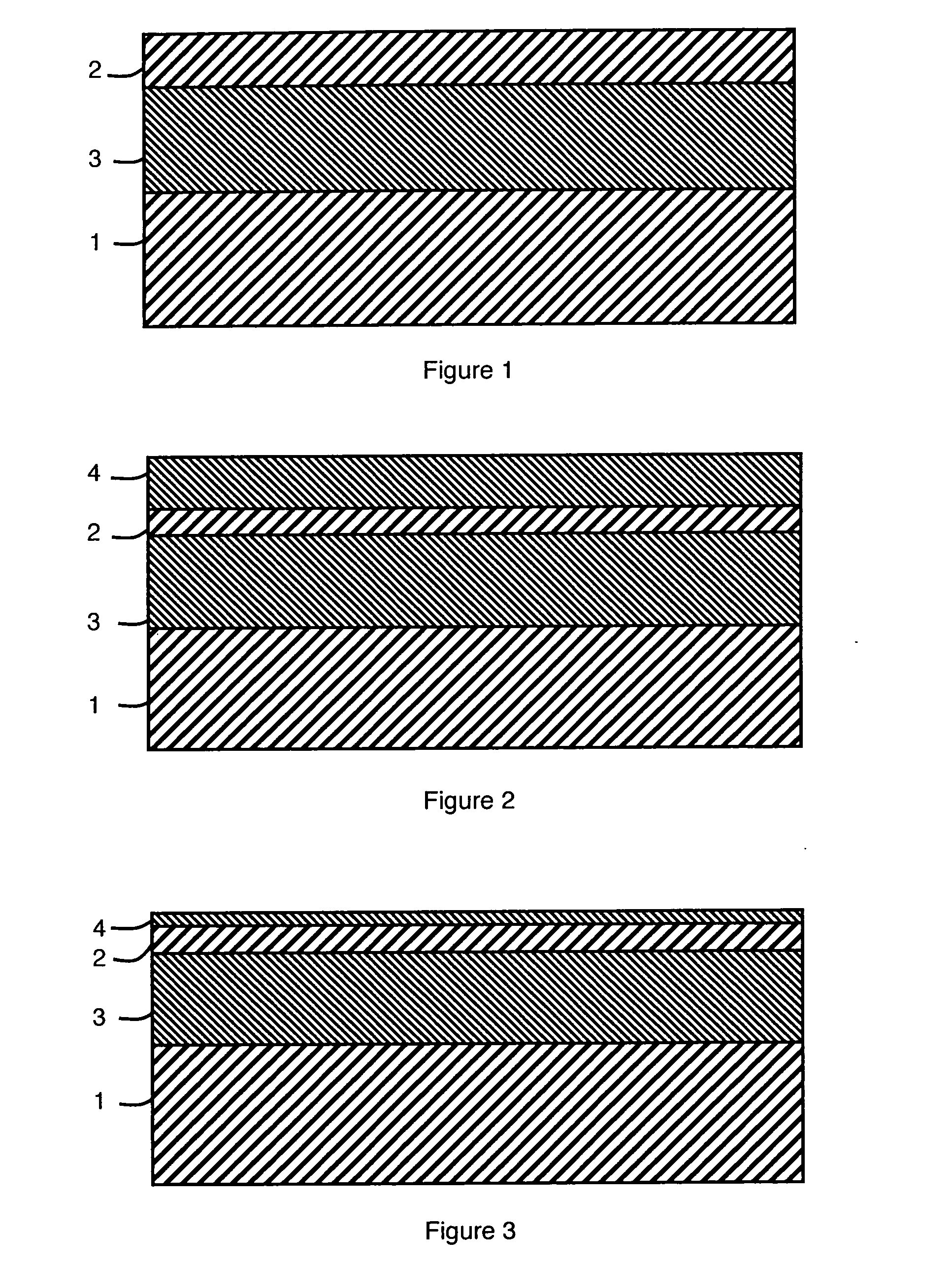
[0039]As represented in FIG. 1, fabrication of the field-effect transistor in conventional manner uses a base substrate constituted by forming a film 2 of conductor material on a buried insulator 3 on a first substrate 1 constituting a mechanical support substrate. First substrate 1 is for example made from bulk silicon and film 2 is formed by a thin layer (for example with a thickness of 50 to 200 nm) of silicon, germanium or SiGe so as to form a silicon on insulator (SOI), germanium on insulator (GeOI), or SiGe on insulator (SiGeOI) base substrate. Buried insulator 3 is for example formed by a buried oxide layer with a thickness of 100 to 400 nm. This base substrate which is available on the market is not necessarily produced at the same time as fabrication of the transistor.

[0040]Film 2 is then preferably thinned, conventionally by oxidation (formation of an oxide layer 4, as represented in FIG. 2) and de-oxidation (as represented in FIG. 3). For gate lengths of less than 20 nm, ...


PUM


Abstract

A first gate, formed on a substrate, is surmounted by a hard layer designed, with first spacers surrounding the first gate, to act as etching mask to bound the channel and a pad that bounds a space subsequently used to form a gate cavity. The hard layer is preferably made of silicon nitride. Before flipping and bonding, a bounding layer, preferably made of amorphous silicon or polysilicon, is formed to bound drain and source areas. After flipping and bonding of the assembly on a second substrate, a second gate is formed in the gate cavity. At least partial silicidation of the bounding layer is then performed before the metal source and drain electrodes are produced.

Description

BACKGROUND OF THE INVENTION[0001]The invention relates to a method for producing a field-effect transistor of planar structure, with double self-aligned gates on each side of a channel and source and drain electrodes, comprising formation of a first gate on a first substrate of semi-conductor on insulator type, deposition on the first gate of a hard layer designed to act as etching mask to bound the channel and a pad that bounds a space subsequently used to form a gate cavity, flipping and bonding of the assembly on a second substrate and formation of a second gate in the gate cavity, photolithographic steps relating to definition of the gates, source and drain areas and channel areas being performed before bonding.STATE OF THE ART[0002]Various methods exist for fabricating double gate field-effect transistors (DGFET) of planar structure. In this type of transistor, preferably achieved on a silicon on insulator (SOI) substrate, first and second gates are respectively arranged on eac...

Claims


Application Information

Patent Timeline
Patent Type & Authority Applications(United States)
IPC IPC(8): H01L21/336
CPCH01L29/458H01L29/66553H01L29/66772H01L27/1266H01L29/78654H01L29/78684H01L29/78648
Inventor LICITRA, CHRISTOPHEPREVITALI, BERNARD
Owner COMMISSARIAT A LENERGIE ATOMIQUE ET AUX ENERGIES ALTERNATIVES
Why Eureka
Try Eureka