
Highly accurate switched capacitor DAC

a switched capacitor and high-accuracy technology, applied in the field of analog circuit design, can solve the problems of linearity errors of multi-bit d/s converters, directly affected by the accuracy of their internal dacs, and its use is typically restricted to low-bit dacs, so as to minimize even-order errors, improve accuracy, and reduce power consumption.

Active Publication Date: 2005-08-02
MICROCHIP TECH INC
View PDF20 Cites 49 Cited by
  • Summary
  • Abstract
  • Description
  • Claims
  • Application Information

AI Technical Summary

Benefits of technology

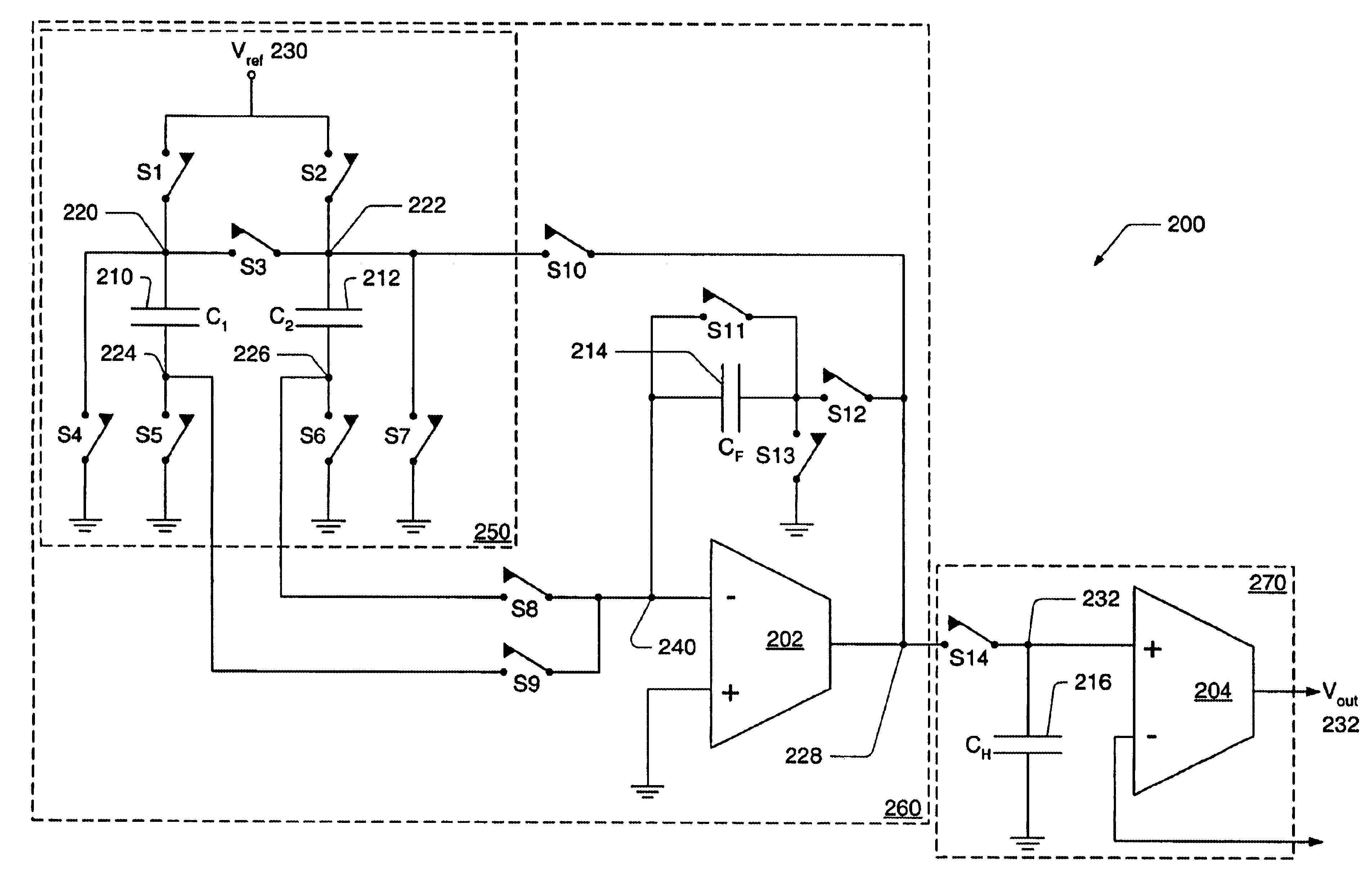
[0016]In one set of embodiments the invention comprises a system and method for designing and operating a highly accurate, low-power, compact size DAC. The charge redistribution technique first introduced by Suarez et al in the IEEE publication “All-MOS Charge Redistribution Analog-to-Digital Conversion Techniques—Part II”, IEEE Journal of Solid State Circuits, Vol. SC-10, No. 6, December 1975, may be employed, where charge redistribution may be performed a first time and again a second time in a complementary fashion, followed by a summing of the two charge distributions, in effect canceling the odd order capacitor mismatch errors. In other words, two complementary conversions may be performed and added together to form a final DAC output voltage. The two complementary conversions, when added, may cancel all odd order mismatch errors such that the accuracy of the DAC may become a function of the square of the mismatch of the two capacitors, resulting in greatly increased accuracy. When performing the complementary conversions for multiple bits, the sequence in which each of the two capacitors is charged may be determined to minimize the even-order errors, especially second-order errors. The invention also proposes applying the DEM technique in conjunction with the complementary conversions, thus substantially reducing even-order errors in addition to eliminating odd-order errors, with less oversampling than required by current DEM implementations.
[0017]Without the proposed canceling, capacitors matched to 0.1% would allow for a resolution of 11 bits, while applying the proposed technique may result in capacitors matched to 0.1% allowing for resolutions of up to twenty-two bits. Integrating the DEM technique with the complementary conversion technique makes it possible to eliminate first, second, and third order errors of a DAC operating with eight times oversampling for up to six bits. D / S multi-bit quantizers may typically use DACs with resolution of less than or equal to six bits. This implies that an accuracy of forty-four bits may be possible with capacitors matching to 0.1%, and any error contributed by capacitor mismatch may be eliminated, though final DAC accuracy will be limited by other error sources in the DAC. The performance of D / S DACs and ADCs may thus also be greatly improved.

Problems solved by technology

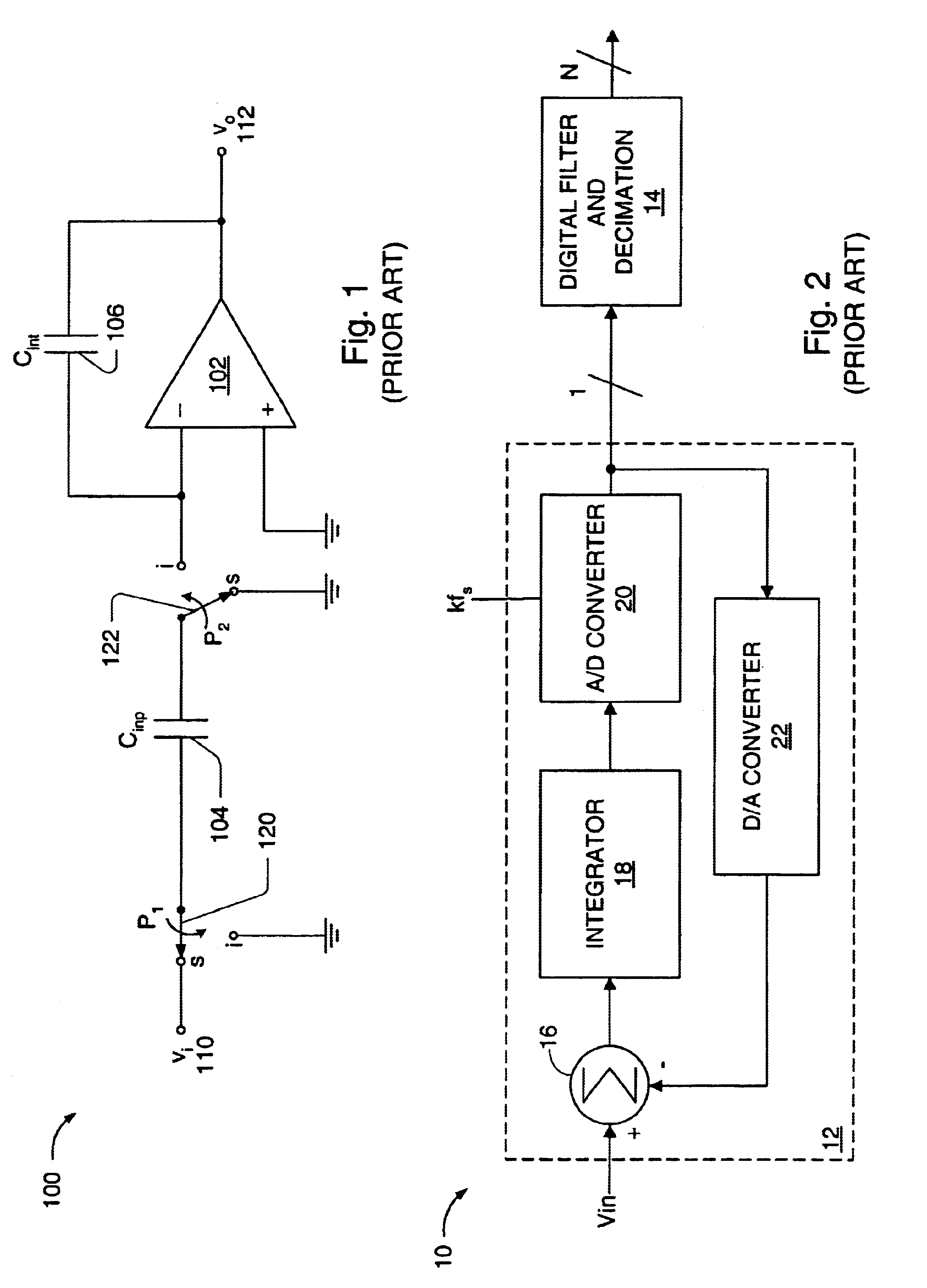
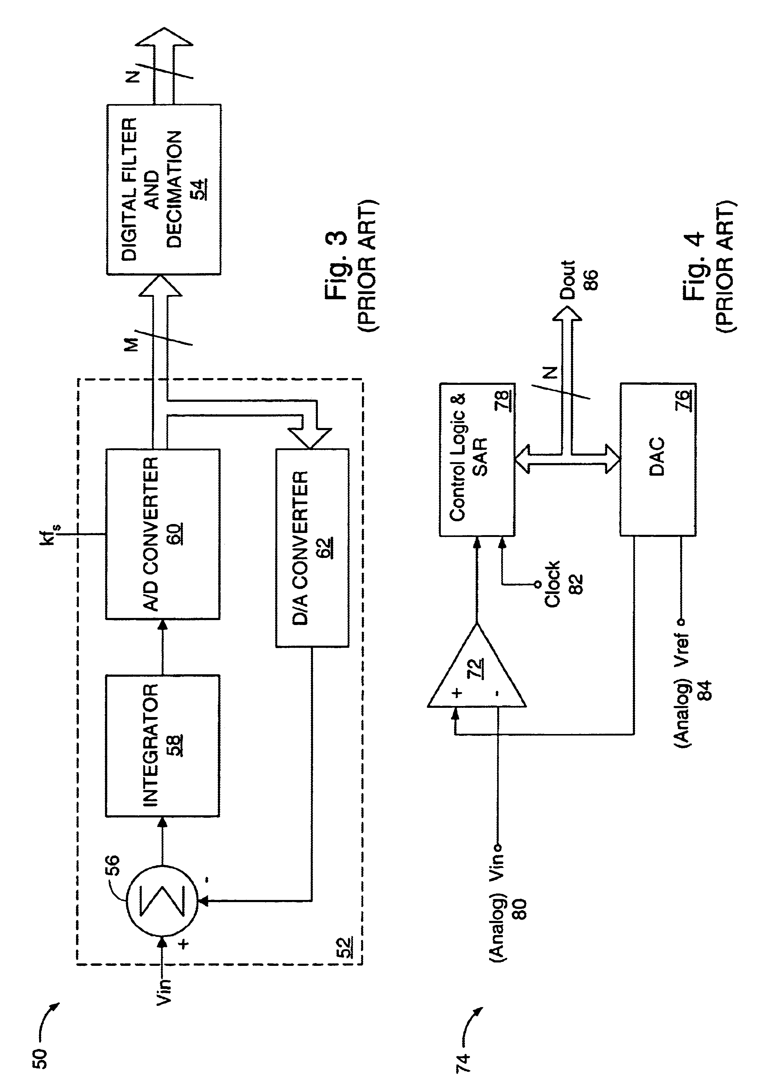
However, multi-bit D / S converter 50 suffers from linearity errors introduced by internal multi-bit DAC 62.
Linearity error is due to the inability of the multi-bit DAC to accurately translate a digital input value into an analog current or voltage.
Similarly, while SAR converters generally operate at fast speeds and typically feature lower complexity and low power consumption, they are also directly affected by the accuracy of their internal DAC.
In other words, one drawback of the DEM technique is that its use is typically restricted to low bit DACs since it requires a unit capacitor for each LSB of the DAC.
Though systems with resolutions of up to 24-bits have apparently been achieved using this technique, the linearity of such systems is difficult to verify.
The drawback of D / S based design lies in the complexity of the DEM technique itself and the complex analog output filter it typically requires.
Previously, capacitor DAC accuracy has been limited to the physical matching obtainable on silicon, which is approximately 0.1% (11 bits).
A significant limitation of this technique lies in its susceptibility to a mismatch error between the two capacitors.

Method used


Image

  • Highly accurate switched capacitor DAC
  • Highly accurate switched capacitor DAC
  • Highly accurate switched capacitor DAC

Examples


Embodiment Construction

[0027]As used herein, when referencing a pulse of a signal, a “leading edge” of the pulse is a first edge of the pulse, resulting from the value of the signal changing from a default value, and a “trailing edge” is a second edge of the pulse, resulting from the value of the signal returning to the default value. A first signal is said to be “corresponding” to a second signal if the first signal was generated in response to the second signal. When data is said to be “registered” or “latched”“using” a signal, the signal acts as a trigger signal that controls the storing of the data into the register or latch. In other words, when a signal “used” for registering or latching data is in its triggering state, the data residing at respective input ports of the register or latch is stored into the register or latch. Similarly, when data is latched “on the leading edge” or “on the trailing edge” of a pulse of a clock, the data residing at respective input ports of a register or latch is stor...


PUM


Abstract

In one set of embodiments the invention comprises a highly accurate, low-power, compact size DAC utilizing charge redistribution techniques. Two complementary conversions may be performed and added together to form a final DAC output voltage by performing charge redistribution a first time, and again a second time in a complementary fashion, followed by a summing of the two charge distributions, in effect canceling the odd order capacitor mismatch errors. By canceling all odd order mismatch errors the accuracy of the DAC may become a function of the square of the mismatch of the two capacitors, resulting in greatly increased accuracy. When performing the complementary conversions for multiple bits, the sequence in which each of the two capacitors is charged may be determined to minimize the even-order errors, especially second-order errors. The DEM technique may be applied, in conjunction with the complementary conversions, with less oversampling than required by current DEM implementations, resulting in even-order errors being substantially reduced in addition to all odd-order errors being eliminated.

Description

BACKGROUND OF THE INVENTION[0001]1. Field of the Invention[0002]This invention relates generally to the field of analog circuit design and, more particularly, to Digital to Analog Converter (DAC) design.[0003]2. Description of the Related Art[0004]Analog-to-digital converters (ADCs) are circuits used to convert signals from the analog domain, where the signals are typically represented by continuous quantities such as voltage and current, to the digital domain, where the signals are generally represented by discrete quantities such as numbers. Similarly, Digital-to-Analog converters (DACs) are circuits used to convert signals from the digital domain to the analog domain. These circuits can be implemented in a variety of ways. Well known and often used conversion techniques include flash, delta-sigma (or sigma-delta), sub-ranging, successive approximation, and integrating.[0005]One often-utilized basic building block of an ADC is the analog integrator, commonly implemented as a switc...

Claims


Application Information

Patent Timeline
IPC IPC(8): H03M1/06H03M3/00H03M1/80H03M1/66H03M1/74H03M3/04
CPCH03M1/066H03M1/804H03M1/466H03M3/464H03M3/502
Inventor MCLEOD, SCOTT C.BASHAR, ANIRUDDHA
Owner MICROCHIP TECH INC
Learn More