Contact sheet and socket including same
- Summary
- Abstract
- Description
- Claims
- Application Information
AI Technical Summary
Benefits of technology
Problems solved by technology
Method used
Image
Examples
first embodiment
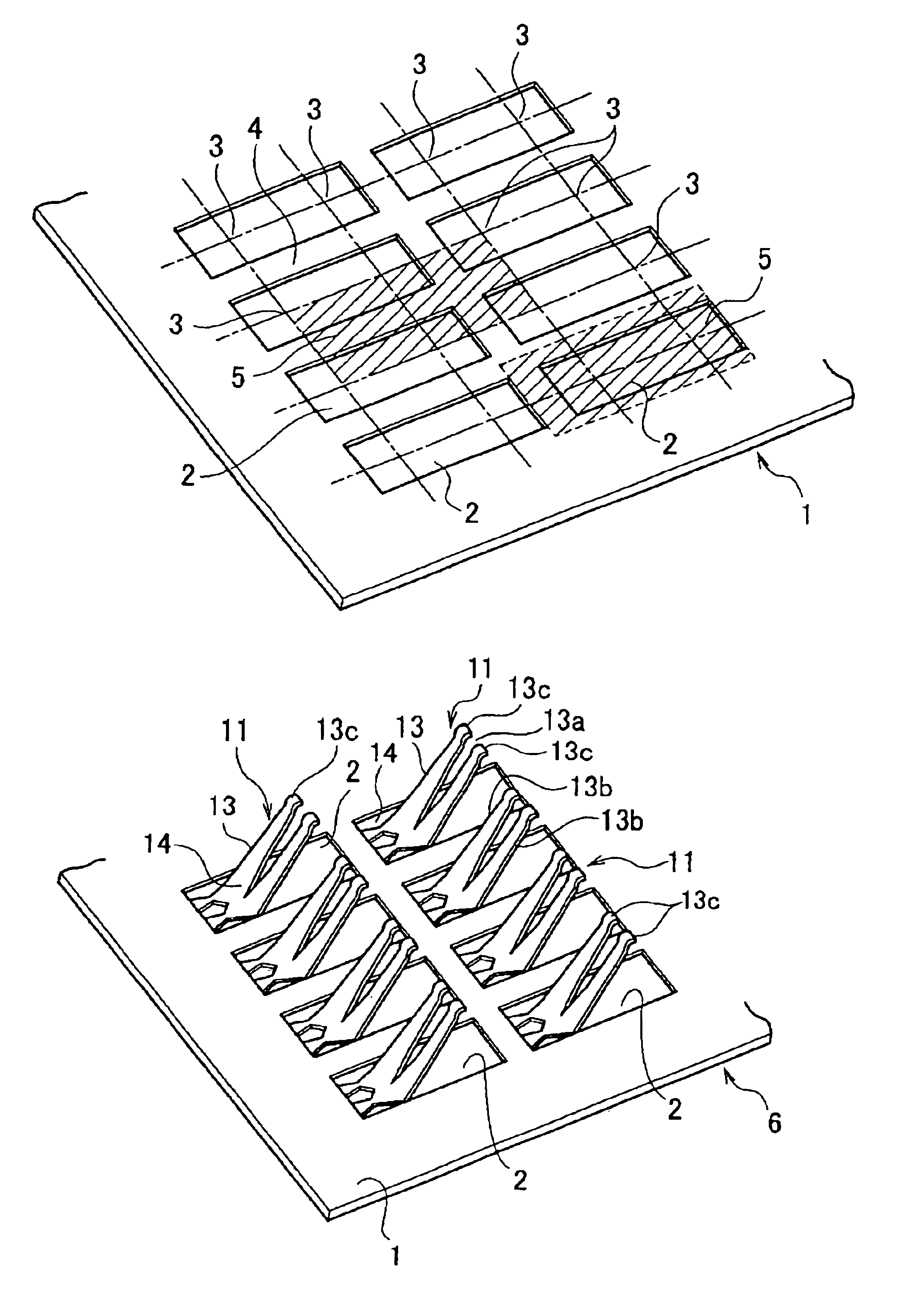
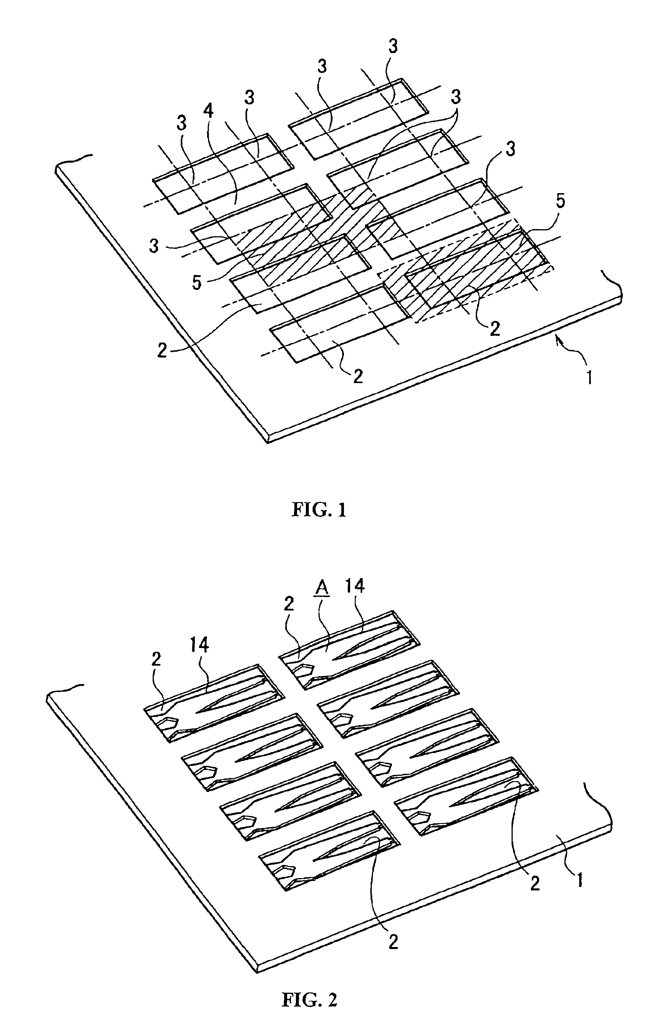
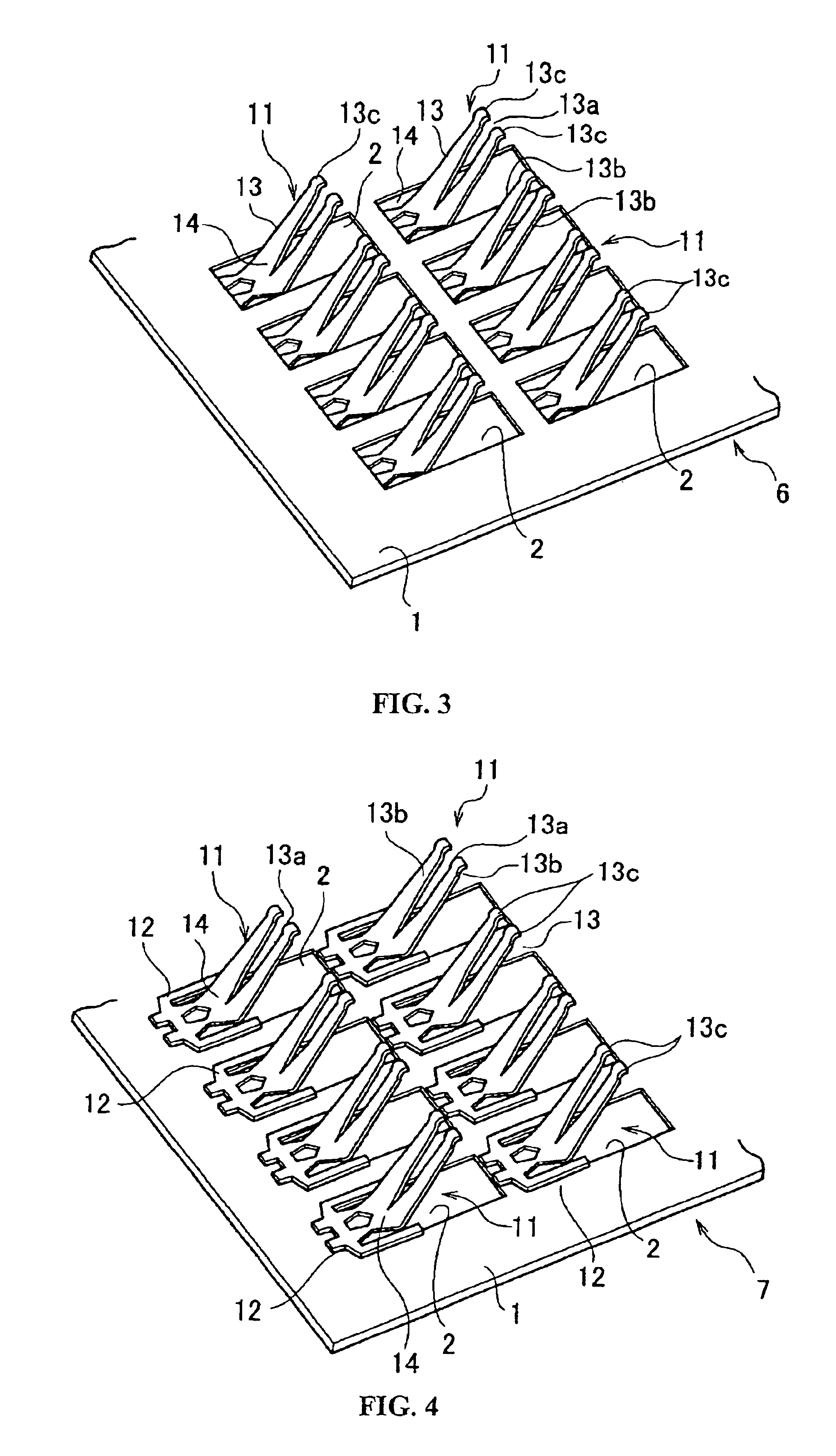
[0053]In FIGS. 1-6, the manufacturing process of a first embodiment of the present invention is shown. FIG. 1, FIGS. 2 and 3 and FIG. 4 respectively show the forming process of the base sheet, the forming process of the first bonded sheet, and the forming process of the second bonded sheet. FIG. 5 and FIG. 6 show a contact sheet and the bonding process for forming the contact sheet, respectively.
[0054]The base sheet 1 is made of a polyimide film. As shown in FIG. 1, the base sheet 1 has a plurality of through-holes 2 formed therein in an arrayed pattern. The square measure of the area of the through-hole 2 and the fixed part 12 of the contact 11 (see FIG. 4) is greater than the unit grid area formed by the arrangement of terminals (not shown) of the electronic device. That is, the amount of the square measure of the through-hole 2 and the fixed part 12 is configured to be larger than that of the unit grid area.
[0055]In FIG. 1, the reference number 3 indicates a center position of a ...
second embodiment
[0073]FIGS. 10-14 show a contact sheet in accordance with a second embodiment of this invention. In this embodiment, a through-hole 2 is formed in a base sheet 1 in a predetermined pattern and configured to correspond to a rectangle consisting of four contiguous unit grids which are formed by an arrangement of the terminals of an electronic device, which is shown as the hatched area 5 in FIG. 10. The through-hole 2 is formed by punching, laser cutting, etching with photosensitive film or any other suitable cutting method. An adhesive layer is formed on one side of the base sheet 1 by coating, either before or after forming the through-hole 2.
[0074]Meanwhile, a metal contact sheet consisting of a plurality of adjacent contacts connected to one another is produced by etching or punching a metal sheet as described above with respect to the first embodiment. In this metal contact sheet, a fixed part of the contact is configured so that the area overlapping the edge portion of the throug...
third embodiment
[0081]FIGS. 15-18 show a contact sheet in accordance with a third embodiment of the present invention.
[0082]In this embodiment, the through-hole 2 is configured as a square having a size that corresponds to a square consisting of four unit grids 4 which are formed by an arrangement of the terminals of an electronic device as shown in FIG. 15. Accordingly, the length of a side of the square through-hole 2 corresponds to twice the length of the side of the unit grid 4. Adopting such dimensions not only makes it easy to form the through-hole 2 but also enlarges the square measure width of a contact to be disposed therein and enables a corresponding increase in spring load.
[0083]FIG. 16 shows a base sheet 1 bonded with a metal contact sheet comprising a plurality of contacts 21. Each contact 21 comprises a fixed part (not shown) and a moving part including a second part 22 contiguous with the fixed part and a third contact portion 23 contiguous with the second part. The fixed part is fi...
PUM
| Property | Measurement | Unit |
|---|---|---|
| Length | aaaaa | aaaaa |
| Electrical conductor | aaaaa | aaaaa |
| Area | aaaaa | aaaaa |
Abstract
Description
Claims
Application Information


