Method for manufacturing flat image display and flat image display

a technology for flat panel displays and flat panels, which is applied in the manufacture of electrode systems, electric discharge tubes/lamps, and tubes with screens, etc. it can solve the problems of inability to effectively absorb gases released in the image display area, the short circuit of wiring may be suppressed, and the exhaust efficiency of the flat panel display is extremely excellent. , the effect of large exhaust conductan

Inactive Publication Date: 2005-08-09
KK TOSHIBA
View PDF15 Cites 9 Cited by
  • Summary
  • Abstract
  • Description
  • Claims
  • Application Information

AI Technical Summary

Benefits of technology

[0015]In the present method for manufacturing the flat panel display, preceding the formation of the getter film, heating / deaerating the faceplate is preferably implemented. By implementing the heating / deaerating, gaseous components in the faceplate can be removed, an intended vacuum in the flat panel display being easily attained. Furthermore, it is preferable to implement the heating / deaerating the rear plate prior to the hermetically sealing. Due to the heating / deaerating, gaseous components in the rear plate can be driven out. In combination with the aforementioned heating / deaerating of the faceplate, the intended vacuum in the flat panel display can be furthermore easily realized.
[0022]In the present invention, first on the faceplate where the phosphor layer is formed on the substrate the getter film is formed. Thereafter, the faceplate thereon the getter film is deposited and the rear plate having the electron source are disposed faced to each other so as to form a gap therebetween, followed by hermetically sealing the gap. Thereby, after manufacturing the display, flashing of the evaporable getter material (getter film formation process) such as Ba alloy or the like can be omitted. The getter film is not deposited on the electron source or the like that does not require the getter film. By implementing the aforementioned processes each in a vacuum to prevent the getter film from being oxidized, the flat panel display having the getter film formed of an active Ba film or the like can be manufactured with reproducibility.
[0028]The present flat panel display has the active getter film (the getter film essentially made of Ba, for instance) formed only on a prescribed position. Thereby, during manufacture or use of the display, the getter film may be suppressed from sticking to a position such as the electron source or the like that does not necessitate the getter film. As a result, short-circuiting of the wiring may be suppressed from occurring. Furthermore, a function as the getter film does not deteriorate during manufacture or use of the display. Accordingly, a vacuum of 10−5 Pa or better can be obtained with reproducibility, and furthermore such vacuum state being maintained over a long period.
[0029]Furthermore, the hermetic sealing is implemented in a vacuum atmosphere, thereby after manufacture of the flat panel display exhausting and vacuuming are made unnecessary. Accordingly, a configuration for exhaust such as a tubing for exhaust for instance, furthermore an exhaust device, which are indispensable in the manufacture of the existing display, are made unnecessary. By dispensing with the tubing for exhaust, exhaust conductance can be made larger, exhaust efficiency of the flat panel display being made extremely excellent.
[0030]The present flat panel display is manufactured based on the aforementioned manufacturing method of the present invention, thereby the aforementioned effect may be obtained.

Problems solved by technology

As a result, when an amount of gas comparable with that of the CRT is released, a pressure increase in the vacuum vessel becomes extremely high.
However, the getter material, being electrically conductive, from a point of view of preventing short-circuit of wiring or the like, is restricted in positions to deposit.
However, in such method of disposing the getter film, the getter film formed at the periphery cannot effectively absorb gases released in the image display area.
Accordingly, a high vacuum in the vacuum vessel cannot be maintained over a long period.
As a result, the getter material is inevitably oxidized in its surface.
Since the getter material is particularly important of its degree of surface activity, the getter material oxidized in its surface cannot exhibit a satisfying gas adsorption effect.
However, such method cannot effectively activate the getter material.
As a result, at this stage, electron emission characteristics or the like are liable to deteriorate.
Accordingly, in the flat panel displays operating in the neighborhood of room temperature or at a little higher temperature than that, a sufficient getter function cannot be obtained.
However, since the evaporable getter materials are assumed to use as alloy, in the flat panel display that operates in the neighborhood of room temperature or at a little higher temperature than that, sufficient gettering action may not be obtained.
Furthermore, if the Ba were evaporated to deposit itself as a Ba film, it would be extremely difficult to suppress the getter film from sticking onto unnecessary portions.
As a result, short-circuit of wiring or the like is liable to occur.
When the getter material sticks onto such reinforcing plate, there may occur short-circuiting between an electron emitter on a cathode side and a phosphor layer on an anode side to result in an occurrence of broken driver or lighting failure.
However, for that, a particular configuration is required to result in a complication.

Method used


Image

  • Method for manufacturing flat image display and flat image display
  • Method for manufacturing flat image display and flat image display
  • Method for manufacturing flat image display and flat image display

Examples


embodiment 1

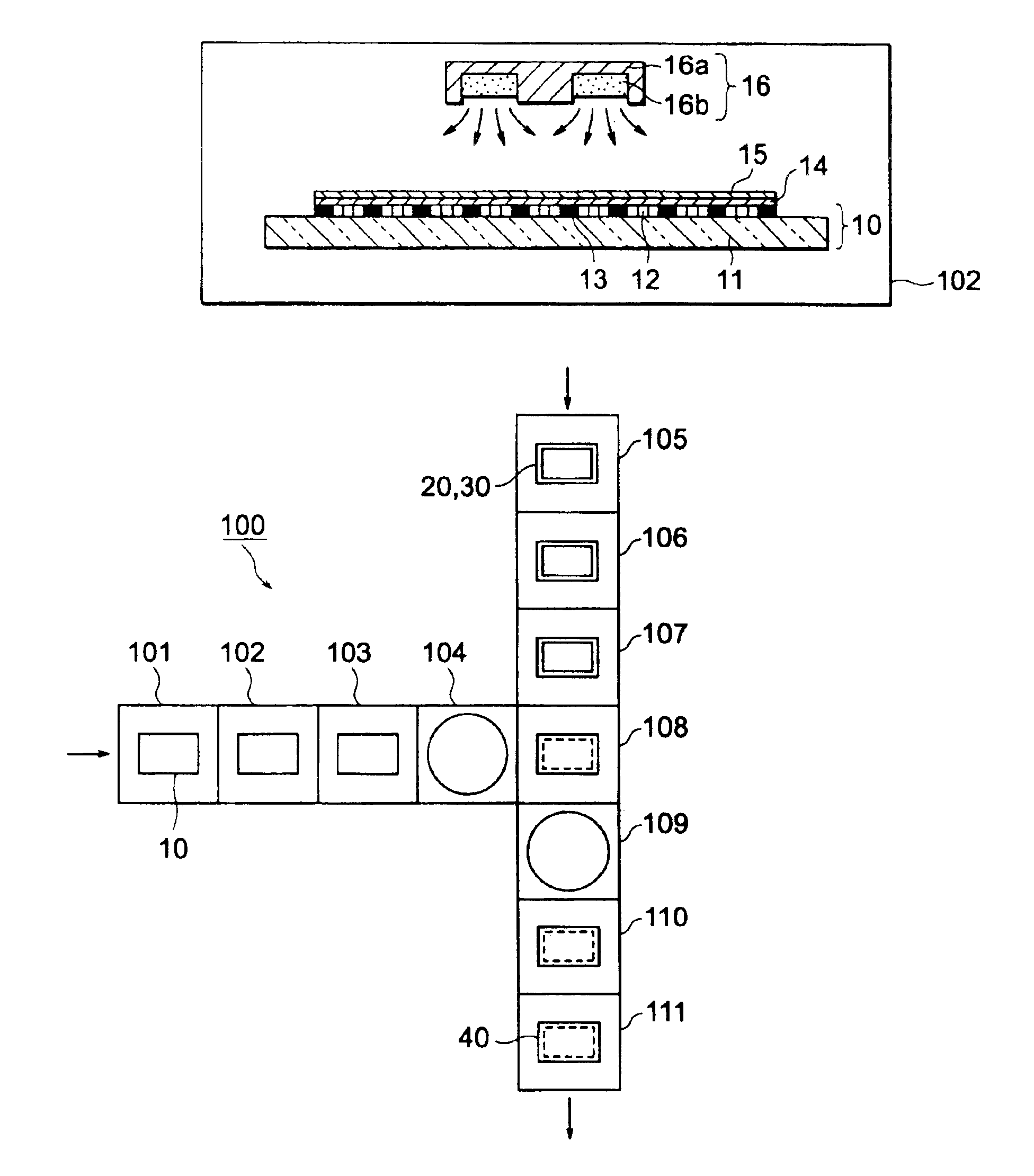
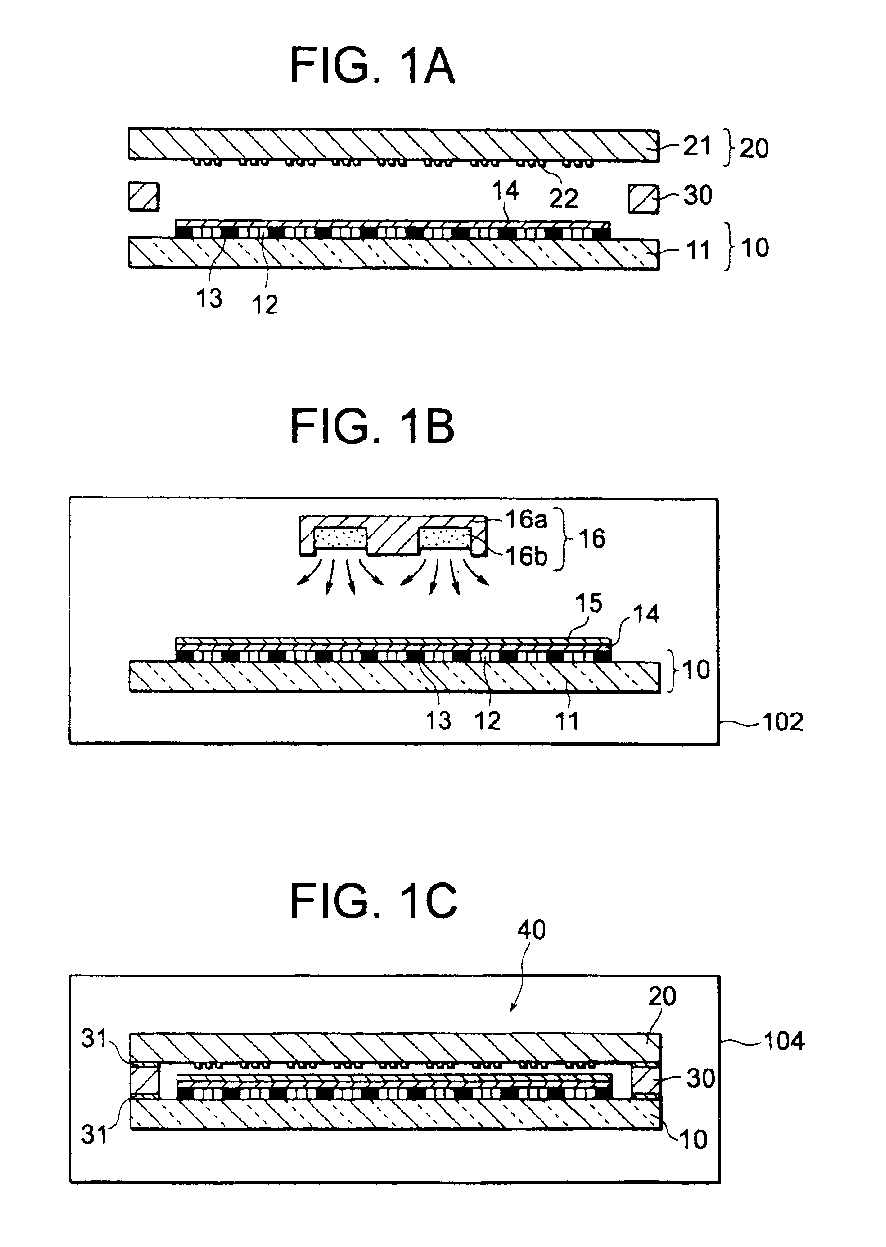
[0079]First, in the vapor deposition chamber 104 of the vacuum treatment apparatus 100 shown in FIG. 3, the faceplate thereon up to the metal back is formed is set at a lower portion thereof. At the same time, at a position of an upper portion thereof facing the metal back the getter device is disposed. For the getter device, one in which getter material of 300 mg containing 48.5% by weight of BaAl4 alloy powder, 50.5% by weight of Ni powder and 1.0% by weight of iron nitride powder is filled in an annular stainless steel getter container with one open end is used. The inside of the vapor deposition chamber 104 is evacuated down to a vacuum of 2×10⁻⁴ Pa.

[0080]Next, the aforementioned getter device is heated from the outside by means of an induction heater to flash (getter flash) Ba. Due to the getter flashing, on the metal back the active Ba film of a thickness of approximately 10 μm is deposited.

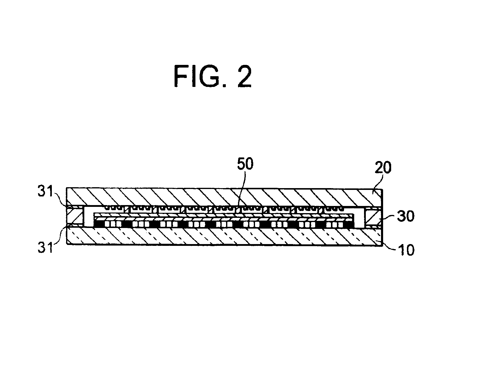
[0081]Next, while maintaining the aforementioned vacuum atmosphere, in the assembly cha...


PUM


Abstract

On a faceplate having a phosphor layer and a metal back that are formed on a substrate, in a vacuum atmosphere, for instance an active Ba film is deposited as a getter film. Following this, while maintaining the vacuum atmosphere, the faceplate thereon the getter film is deposited and a rear plate having a plurality of electron emitters formed on a substrate are oppositely disposed to form a gap therebetween through a support frame, the gap being hermetically sealed. A flat panel display comprises the active Ba film formed on for instance the metal back as a getter film. Such getter film, while maintaining an activity, is disposed on an image display region in a vacuum vessel, having an excellent getter function.

Description

FIELD OF THE INVENTION[0001]The present invention relates to a method for manufacturing a flat panel display that uses an electron emitter such as a field emission cold cathode or the like, and a flat panel display.DISCUSSION OF THE BACKGROUND[0002]Recently, by the use of for instance advanced semiconductor machining technology, field emission cold cathodes have been under active study and have been forwarded to apply in flat panel displays. A flat panel display comprises a rear plate in which a lot of field emission electron emitters are formed as electron sources on a substrate, and a face plate formed of a glass substrate or the like thereon a phosphor layer is formed. These are oppositely disposed to each other a prescribed gap apart. Such flat panel displays, different from liquid crystal displays, are self-emitting and can dispense with a backlight. Accordingly, on the basis of these, the flat panel displays are characterized in being lower in power consumption, broader of an ...

Claims


Application Information

Patent Timeline
Patent Type & Authority Patents(United States)
IPC IPC(8): H01J29/94H01J29/00H01J9/39H01J9/24H01J9/38H01J9/48
CPCH01J9/241H01J9/39H01J9/48H01J29/94H01J2209/385H01J31/12
Inventor NAKAYAMA, SHOJITAKENAKA, SHIGEO
Owner KK TOSHIBA
Why Eureka
Try Eureka