In recent years, semiconductor devices have become smaller in size and structures of semiconductor elements have become more complicated.
Accordingly, irregularities on a surface of a
semiconductor device become increased, and hence step heights on the surface of the semiconductor device tend to be larger.
Further, an open circuit is caused by disconnection of interconnects, or a
short circuit is caused by insufficient insulation between interconnect
layers.
As a result, good products cannot be obtained, and the yield tends to be reduced.
Furthermore, even if a semiconductor device initially works normally, reliability of the semiconductor device is lowered after a long-term use.
Therefore, if the irregularities of the surface of the semiconductor device are increased, then it becomes difficult to form a fine pattern on the semiconductor device.
In such a
polishing apparatus, if a relative pressing force between the semiconductor
wafer being polished and the polishing surface of the polishing pad is not uniform over an entire surface of the semiconductor
wafer, then the semiconductor wafer may insufficiently be polished or may excessively be polished at some portions depending on the pressing force applied to those portions of the semiconductor wafer.
The polishing pad is so elastic that the pressing force applied to a
peripheral portion of the semiconductor wafer tends to become non-uniform.
Since a conventional substrate holding apparatus, as described above, for uniformly pressing an entire surface of a semiconductor wafer polishes the semiconductor wafer uniformly over the entire surface thereof, it cannot realize a polishing amount distribution that is equal to the aforementioned film thickness distribution on the surface of the semiconductor wafer.
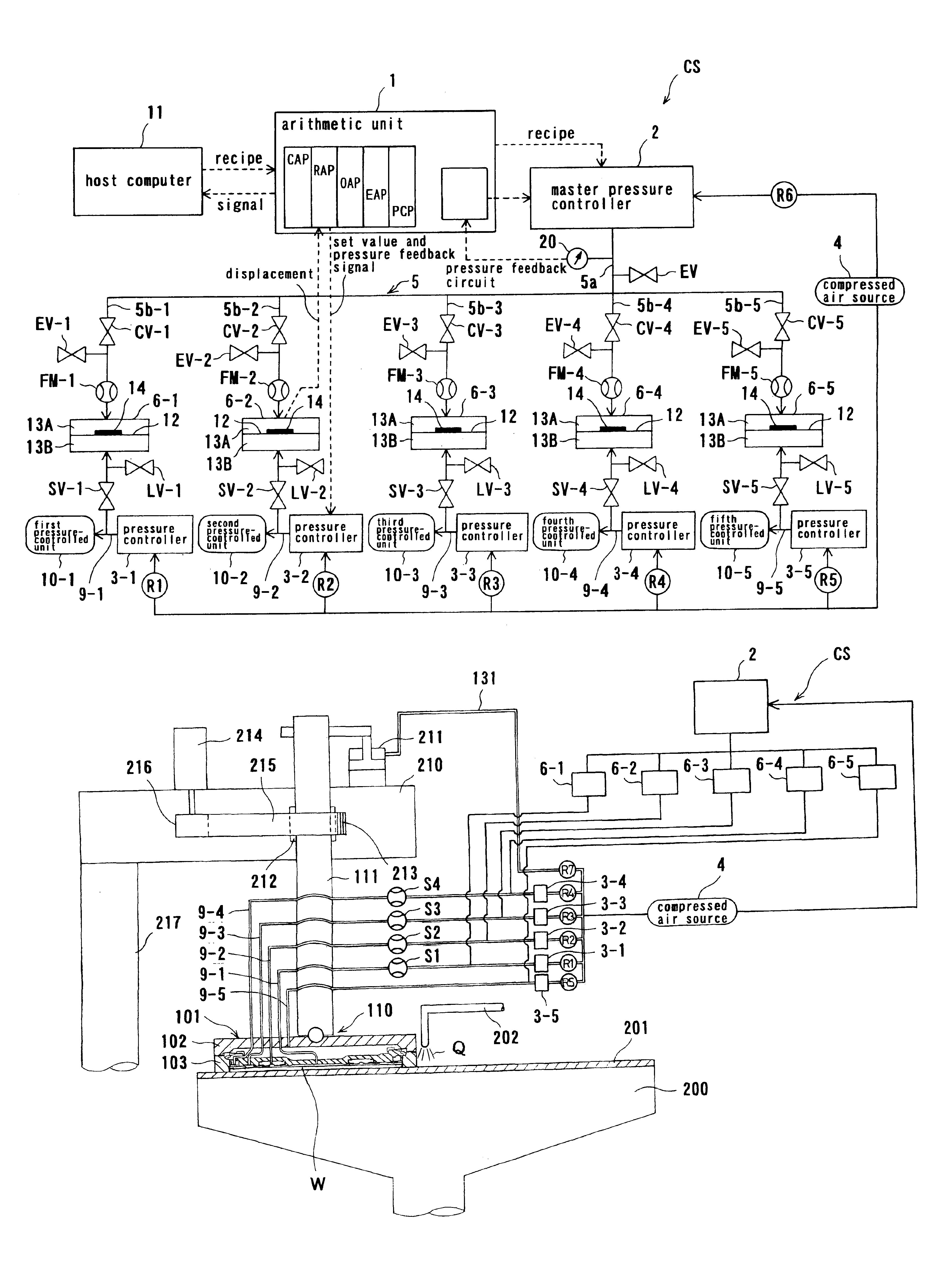
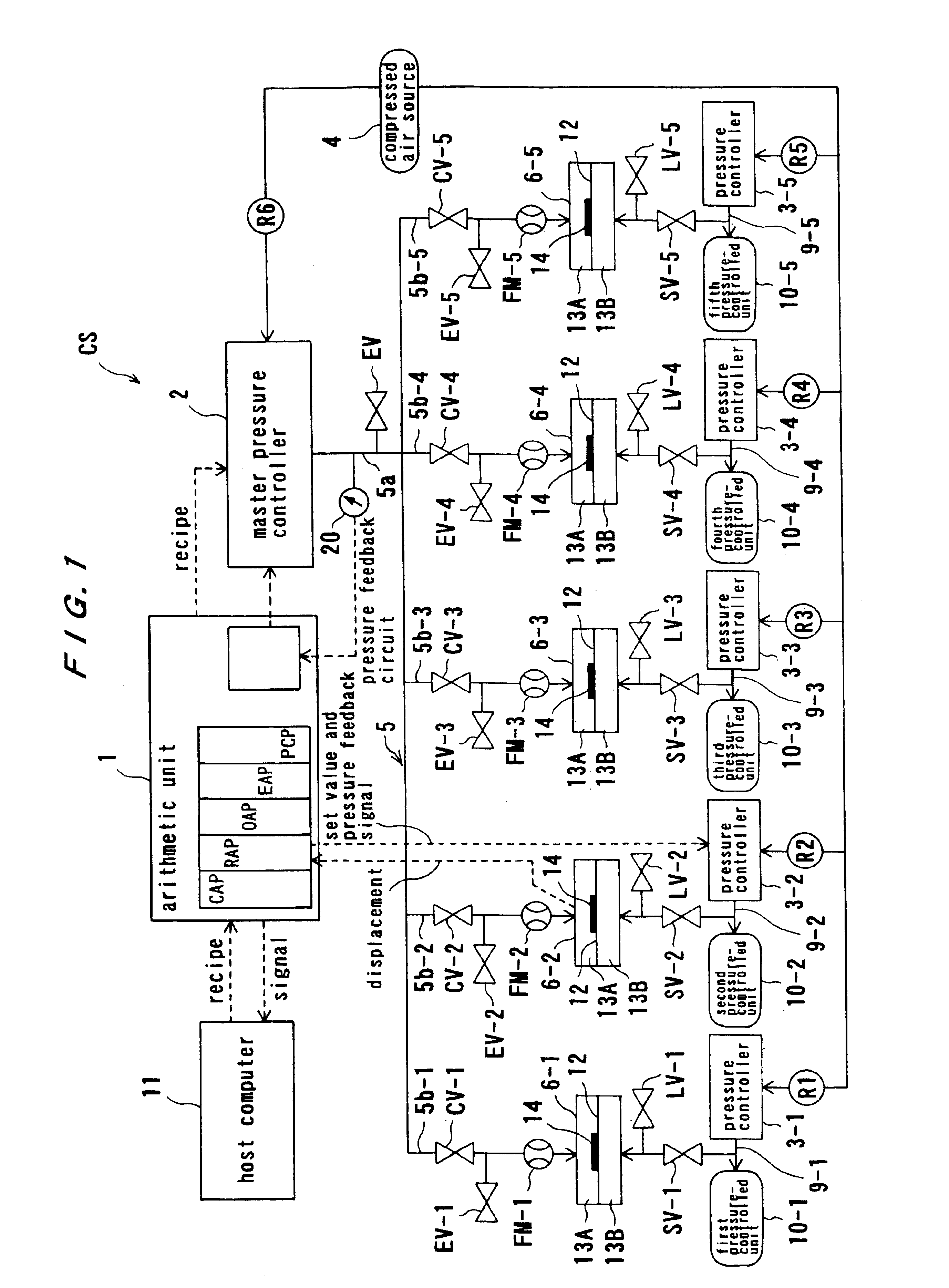
In this case, each of the pressure controllers can perform
feedback control for itself, but cannot perform any control between itself and other pressure controllers.
Specifically, each of the pressure controllers cannot eliminate an individual difference between itself and other pressure controllers.
Therefore, even if the fluid having the same pressure is expected to be supplied to the respective pressure chambers by controlling the respective pressure controllers, the respective pressure chambers cannot be kept at the same pressure because pressures outputted from the respective pressure controllers are different from each other by the individual differences of the pressure controllers.
Accordingly, the semiconductor wafer cannot be polished uniformly over the entire surface thereof.
Further, even if a predetermined
differential pressure is expected to be developed between the two pressure chambers to make a pressing force for pressing a thicker film region on a semiconductor wafer against a polishing surface greater than a pressing force for pressing a thinner film region on the semiconductor wafer against the polishing surface, thereby selectively increasing the polishing rate of the thicker film region, the predetermined differential pressure cannot be developed between the two pressure chambers because pressures outputted from the two pressure controllers are added by pressure errors caused by the individual differences of the pressure controllers.
As a result, the respective zones (regions) of the semiconductor wafer cannot be polished at desired polishing rates.
However, in the case where pressures of a plurality of pressure-controlled sections (or units) are controlled using a plurality of pressure controllers, the same problem arises due to the individual differences of the pressure controllers.
Specifically, pressures of the respective pressure-controlled sections cannot be controlled to desired values owing to the individual differences of the respective pressure controllers.

