Method of manufacturing actuator and ink jet head

a manufacturing method and actuator technology, applied in the field of manufacturing methods of actuators and ink jet heads, can solve the problem that the desired properties of piezoelectric films cannot be formed, and achieve the effect of excellent piezoelectric properties and excellent properties

Inactive Publication Date: 2005-08-09
CANON KK
View PDF7 Cites 39 Cited by
  • Summary
  • Abstract
  • Description
  • Claims
  • Application Information

AI Technical Summary

Benefits of technology

[0014]The manufacturing method of the present invention has an effect that a long, highly dense piezoelectric actuator and ink jet head with excellent properties can be produced. Further, the manufacturing method of present invention has another effect that a piezoelectric film with excellent piezoelectric properties can be selected by means of a single crystal substrate and a device with large dimensions can also be processed.

Problems solved by technology

As a method of manufacturing the long, large area actuator and ink jet head generally employed is such a method that after directly forming a piezoelectric film on a diaphragm structure body a device is fabricated by processing and molding, however there is a case where a piezoelectric film with desired properties cannot be formed with regard to the lattice constant and the thermal expansion coefficient of the diaphragm structure body.

Method used


Image

  • Method of manufacturing actuator and ink jet head
  • Method of manufacturing actuator and ink jet head
  • Method of manufacturing actuator and ink jet head

Examples


example 1

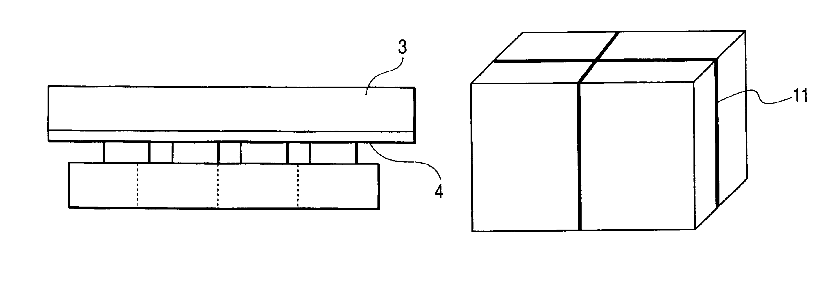
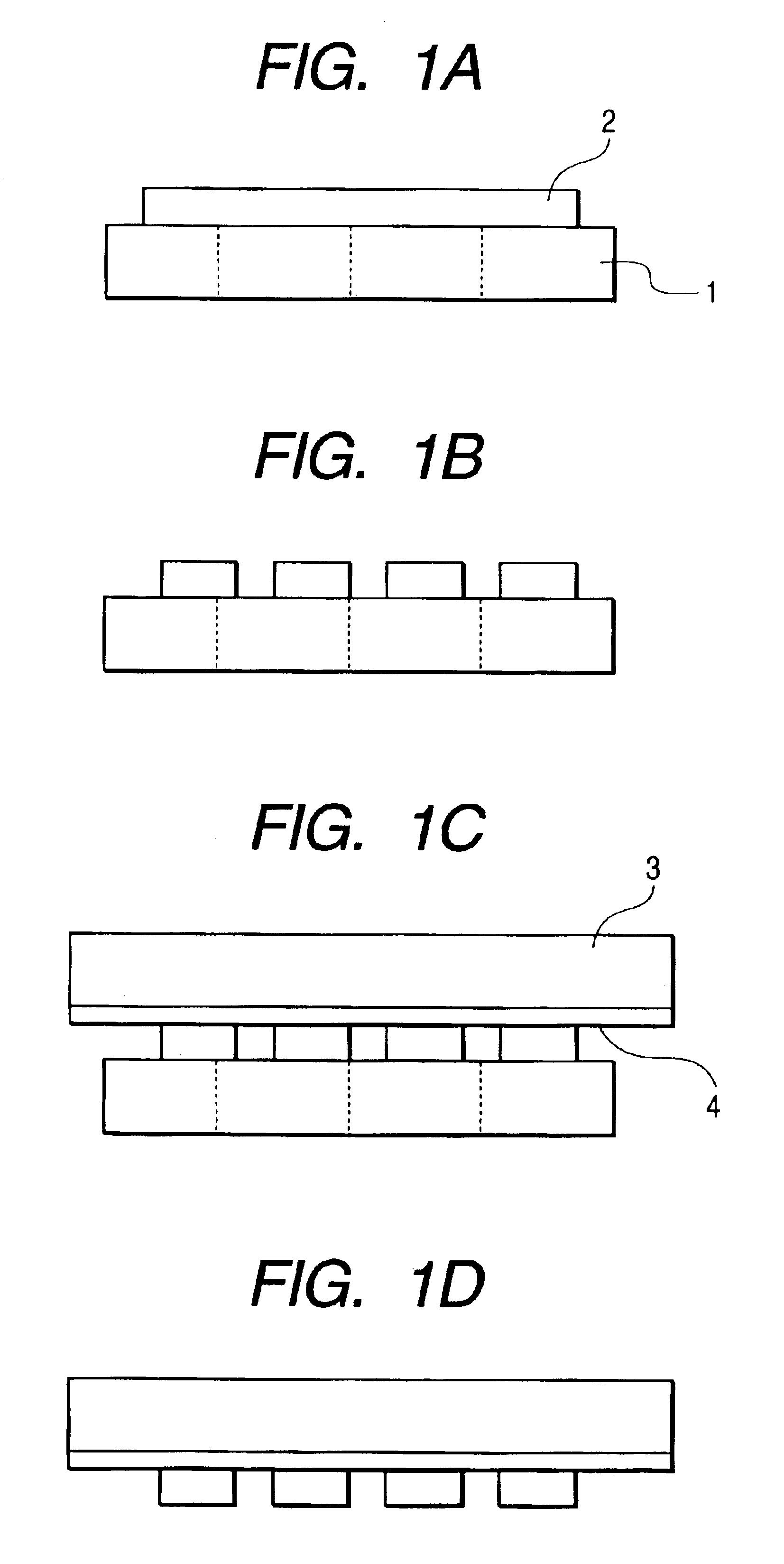
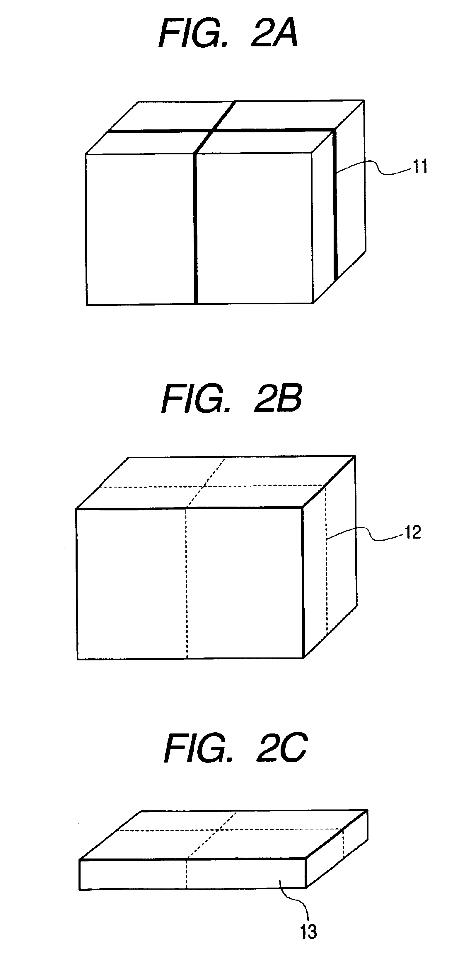
[0037]10 SrTiO3 (100) single crystal cubic bulk bodies with a side of 10 mm were bonded and then cut to form a PZT (001) film of 2.5 μm by a spattering process on the manufactured STO (SrTiO3) substrate with a dimension of 10 mm×100 mm (thickness 0.15 mm, width of a bonded portion 1.2 μm, a surface roughness through the bonded portion Ra=5 nm). The PZT film was a single crystal oriented in the orientation [001]. In a rocking curve measured about the bonded STO substrate by XRD measurement, a peak was recognized at the location 0.13°-0.16° dethroughted from that of the main peak. After forming a Ti layer (20 nm thick) on the PZT film on the STO substrate, a Au layer (200 nm thick) was formed to make a bond layer. These were etched to be as dense as 180 dpi. The size of one PZT element after etching was 88 μm in width, 2.8 mm in length, and 680 pieces of the PZT elements are arranged on the STO substrate.

[0038]Cr (30 nm) and Au (200 nm) was formed as a bond layer on a SOI substrate (R...

example 2

[0040]A patterned body of a piezoelectric film was manufactured in the same manner except that the thickness of the piezoelectric film was chosen as 4 μm, and the piezoelectric films were bonded on both sides of 20 μm thick Ti substrate at the same time. Then, an actuator of bimorph type was obtained by exfoliating an STO substrate. By measuring an amount of displacement with a laser displacement meter by the same method as in Example 1 in the condition where the same voltage was applied to the piezoelectric films on both sides using the Ti substrate as an electrode, the displacement of 1.25 μm at 1 kHz, and of 0.45 μm at 10 kHz was measured. Further, variations between every element were small and excellent properties were shown.

example 3

[0041]After forming PbTiO3 on the bonded MgO substrate (thickness 0.5 mm, width of bonded portion 400 nm or less), a PZT single crystal film was formed thereon. The dethroughtion of orientation of the MgO substrate used in this example was determined by observing two peaks 0.13° apart from each other at the location of the peak of (400) in the rocking curve measured (see FIG. 4). The PZT film on the substrate comprised a 98% or more unidirectionally oriented film according to the ratio of the peak intensities in XRD measurement (θ-2θ measurement). Manufacturing an actuator in the same manner as Example 1 except that PbTiO3 was removed by etching, the actuator with similar good properties was obtained.

[0042]When forming a piezoelectric film in the same manner on a substrate with 0.31° dethroughtion of the orientation in the rocking curve measurement, the PZT film was composed of a 90% unidirectionally oriented film, and the property of an actuator manufactured was poor a little in an...


PUM


Abstract

A method of manufacturing an actuator comprises the steps of bonding a piezoelectric film formed on a single crystal substrate to a diaphragm structure member and removing the single crystal substrate therefrom to manufacture the actuator. The single crystal substrate is a substrate having bonded portions where a plurality of single crystal substrates are bonded together.

Description

BACKGROUND OF THE INVENTION[0001]1. Field of the Invention[0002]The present invention relates to a manufacturing method of an actuator and an ink jet head comprising the steps of bonding a piezoelectric film formed on a single crystal substrate to a diaphragm structure member and removing the single crystal substrate therefrom to manufacture the actuator and ink jet head. Particularly, the present invention relates to a manufacturing method useful for forming the actuator and ink jet head with a large area. Also, the manufacturing method can produce actuators and ink jet heads with large areas.[0003]For example, the method can be suitably employed for manufacturing a piezoelectric / electrostrictive film type element, such as an ink jet print head, microphone, an articulator (loud speaker, etc.), various oscillators and radiators, as well as a piezoelectric / electrostrictive film type element which generates bending displacement of unimorph or bimorph type used for sensors, etc. Beside...

Claims


Application Information

Patent Timeline
Patent Type & Authority Patents(United States)
IPC IPC(8): B41J2/16H01L41/22B41J2/14H01L41/18H01L41/313
CPCB41J2/161B41J2/1623B41J2/1628B41J2/1629B41J2/1632B41J2/1634B41J2/1642H01L41/313H01L41/0973H01L41/314H01L41/33H10N30/2047H10N30/073H10N30/076H10N30/082
Inventor FUKUI, TETSUROMATSUDA, TAKANORIIFUKU, TOSHIHIROIKESUE, AKIO
Owner CANON KK
Why Eureka
Try Eureka