Supercharge Your Innovation With Domain-Expert AI Agents!

Nonvolatile semiconductor memory device

a semiconductor and memory device technology, applied in semiconductor devices, digital storage, instruments, etc., to achieve the effect of reducing the area of the selection transistor portion

Inactive Publication Date: 2005-08-09
RENESAS ELECTRONICS CORP
View PDF9 Cites 9 Cited by
  • Summary
  • Abstract
  • Description
  • Claims
  • Application Information

AI Technical Summary

Benefits of technology

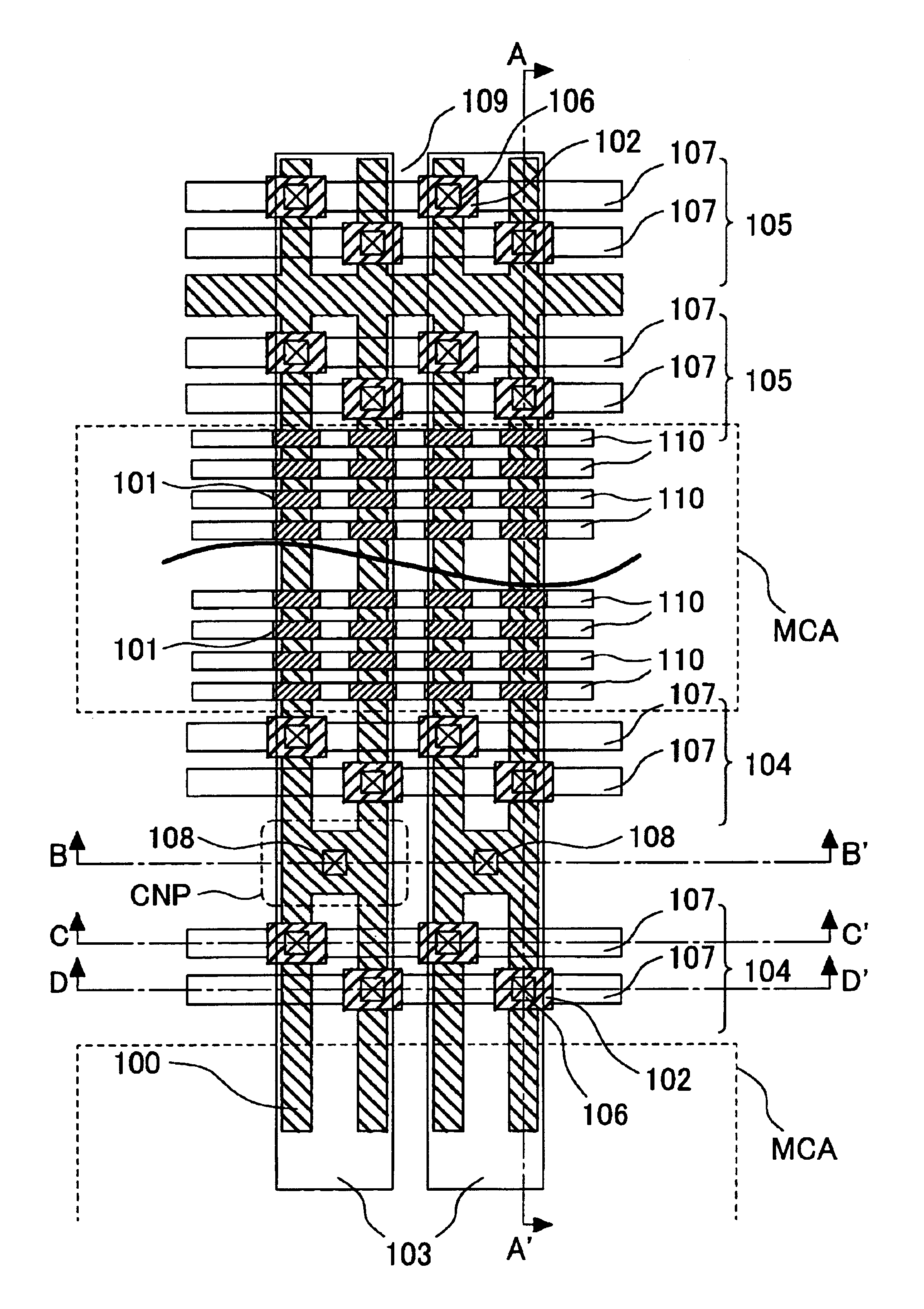
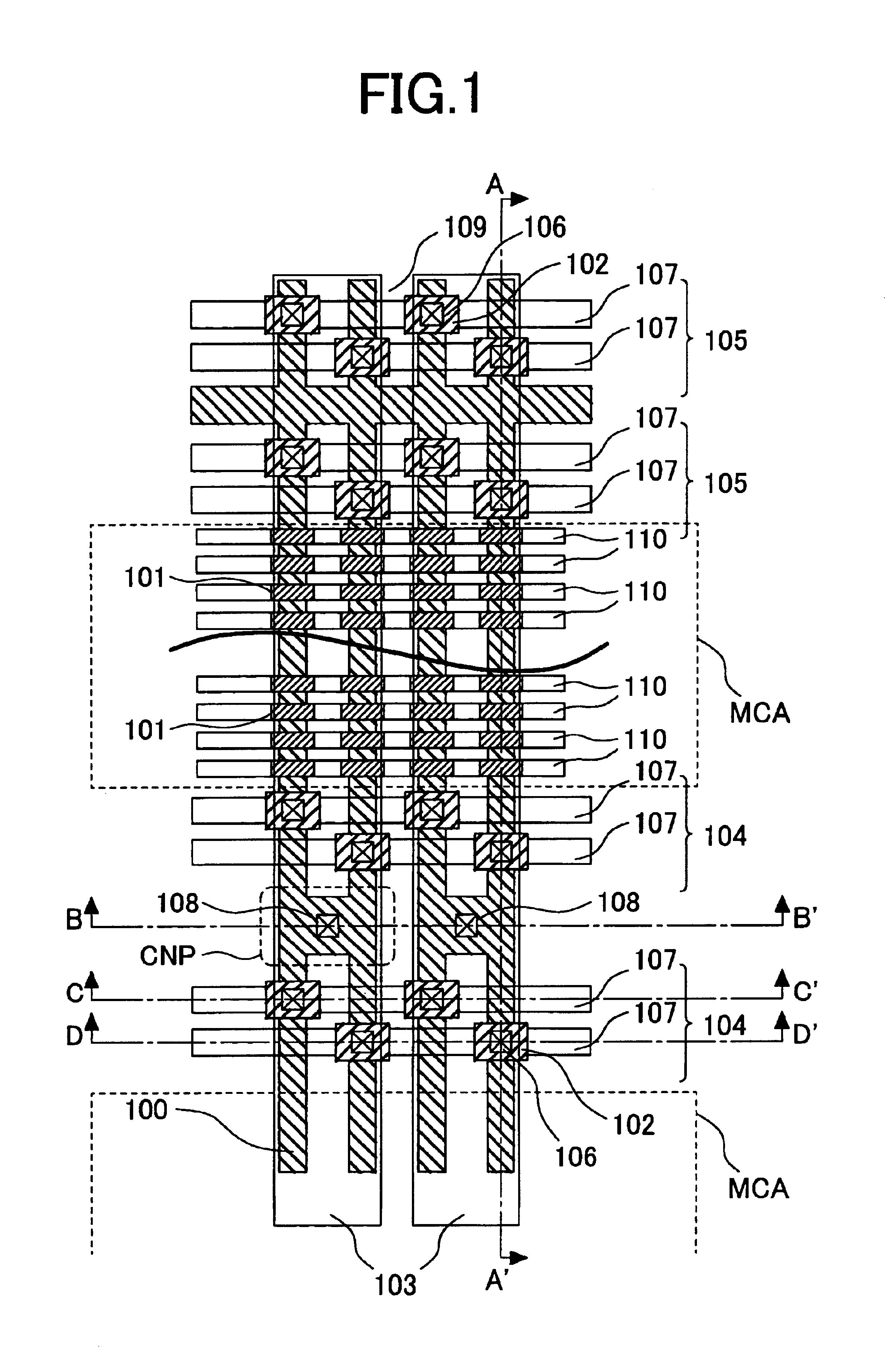
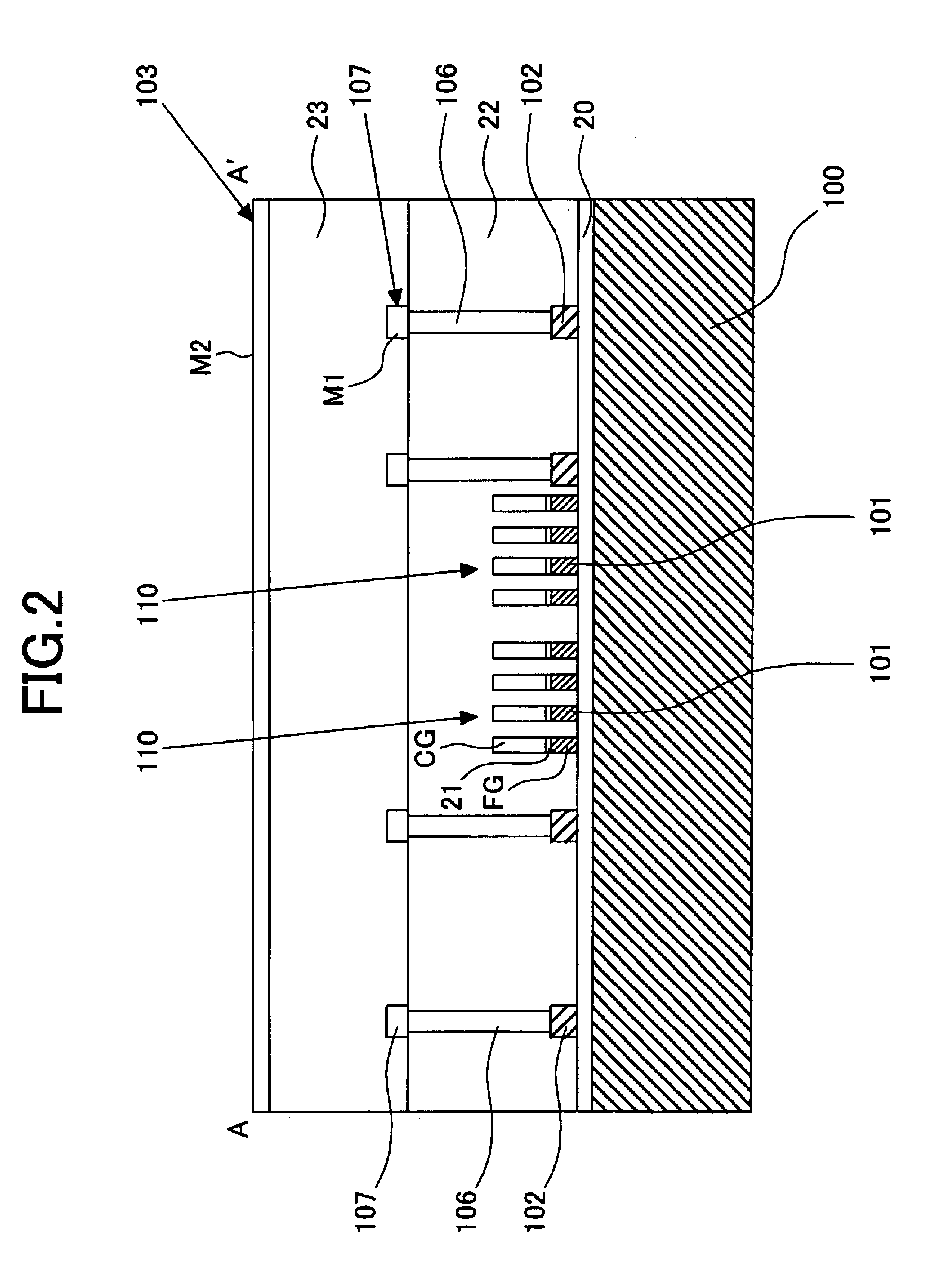
The present invention is about a nonvolatile semiconductor memory device that improves integration degree by reducing the area for the selection transistor portion. The device has a memory cell array with plural nonvolatile memory cells arranged in a matrix. It includes first and second selection transistors for selecting the first and second active regions, which are connected by way of contact holes with global bit lines. The gates of the selection transistors are separated and disposed each by one on the first and second active regions. The contact hole is formed about at the intersection between one of the first and second active regions and the connection portion. The gates of the selection transistors are separated and disposed being further extended from the first active region to the third active region adjacent with the second active region. The memory cells are connected in series or parallel to the global bit line. The nonvolatile memory cell has a first gate, a second gate, and a third gate with different functions. The technical effects of the invention are improved integration degree and efficient selection of active regions for memory cells.

Problems solved by technology

However, in the two patent documents described above, a method of decreasing the area for the selection transistor portion per se is not disclosed.

Method used


Image

  • Nonvolatile semiconductor memory device
  • Nonvolatile semiconductor memory device
  • Nonvolatile semiconductor memory device

Examples


embodiment 2

[0054]Then, Embodiment 2 of the nonvolatile semiconductor memory device according to the invention is to be described with reference to FIG. 8. The difference from Embodiment 1 is that the gates 102 of the selection transistors in the first selection transistor portion 104 is in the mirror symmetry with respect to the connection portion CNP for the active region 100 (that is, line-to-line symmetry with respect to line E-E′), and that the contact hole 108 is formed being displaced from the center for the active connection portion CNP to the intersection between the active region connection portion CNP and the active region 100. Other components, materials, structures are identical with those in Embodiment 1 described previously.

[0055]The structure of the existent selection transistor portion required selection transistors in four stages, alignment margin between the selection transistor and the contact hole and a space for disposing the contact hole. The advantageous feature of the s...

embodiment 3

[0057]Then, Embodiment 3 of the nonvolatile semiconductor memory device according to the invention is to be described with reference to FIG. 9. This embodiment is different from Embodiment 2 in that the adjacent first selection transistor portions 104 are asymmetrical with respect to a plane perpendicular to the global bit line 103 and passing through the center of the connection portion CNP of the active region, and a contact hole 108 is formed at an intersection between the active connection portion CNP and the active region 100. Other components, materials and structures are identical with those in Embodiment 1.

[0058]Thus, the first selection transistor portion 104 can be laid out only with the selection transistor gates 102 in four stages and the area for the selection transistor portion can be decreased compared with Embodiment 1.

[0059]The operation method of the selection transistors in this embodiment is identical with the operation method for the selection transistors in Emb...

embodiment 4

[0060]Then, Embodiment 4 of the nonvolatile semiconductor memory device according to the invention is to be described with reference to FIG. 10.

[0061]This embodiment is different from Embodiment 2 in that gates 102 of the first selection transistor portion 104 are disposed so as to be in common with the two adjacent active regions 100. That is, the separated selection transistor gates are extended from one side of first and second active regions 100-1 and 100-2 to an adjacent third active region 100-3.

[0062]The advantageous feature of this embodiment, when compared with Embodiments 1 to 3, is that the number of contact holes 106 disposed to the gate electrode 107 of the first selection transistor portion 104 and the second selection transistor portion 105 can be decreased thereby enabling to moderate the pitch for the contact holes. Thus, it is possible to suppress lowering of yield caused by contact failure between the gate of the selection transistor and the contact hole. Further,...


PUM


Abstract

A nonvolatile semiconductor memory device improved with integration degree, in which the gate of the selection transistors is separated on each of active regions, first and second selection transistors are arranged in two stages in the direction of the global bit line, the gates for the selection transistors in each stage are disposed on every other active regions, contact holes are formed in mirror asymmetry with respect to line B—B in the connection portion for the active regions, the gate is connected through the contact hole to the wiring, the adjacent active regions are connected entirely in one selection transistor portion and connected in an H-shape for adjacent two active regions in another selection transistor portion, and the contact hole is formed in the connection portion and connected when the global bit line, whereby the pitch for the selection transistor portion can be decreased in the direction of the global bit line.

Description

BACKGROUND OF THE INVENTION[0001]1. Field of the Invention[0002]The present invention relates to a nonvolatile semiconductor memory device and more particularly to a structure of a memory cell array suitable to higher integration of a nonvolatile semiconductor memory device capable of electric rewriting.[0003]2. Description of Related Art[0004]Since a flash memory as one of nonvolatile semiconductor memory devices is excellent in portability, impact resistance and capable of electrically erasing collectively, a demand therefor has been increased rapidly in recent years as a memory device for small-sized portable information equipments such as portable personal computers or portable telephones.[0005]In the flash memory, lowering of the bit cost is an important subject and, for attaining this, there has been proposed a method of decreasing the number of contact holes and global bit lines thereby decreasing the chip area by improving the layout not only for the memory cells but also fo...

Claims


Application Information

Patent Timeline
Patent Type & Authority Patents(United States)
IPC IPC(8): G11C16/04H01L27/115H01L21/8247G11C8/02H01L29/788H01L29/792H10B69/00
CPCG11C16/0408H01L27/115H10B69/00
Inventor ARIGANE, TSUYOSHIKOBAYASHI, TAKASHISASAGO, YOSHITAKA
Owner RENESAS ELECTRONICS CORP
Features
  • R&D
  • Intellectual Property
  • Life Sciences
  • Materials
  • Tech Scout
  • Unparalleled Data Quality
  • Higher Quality Content
  • 60% Fewer Hallucinations
Learn More